
Click on the author name to see the abstract.
Format: A0 portrait.
Poster
NFFA-Europe: enhancing European competitiveness in nanoscience research and innovation
1IOM-CNR Laboratorio TASC, Area Science Park, s.s. 14 km 163.5, Basovizza, 34149 Trieste, Italy
NFFA-Europe is a European open-access resource for experimental & theoretical nanoscience that carries out comprehensive projects for multidisciplinary research at the nanoscale, ranging from synthesis to nano-characterization, to theory and numerical simulation. Advanced infrastructures specialized on growth, nano-lithography, nano-characterization, theory and simulation and fine-analysis with Synchrotron, FEL and Neutron radiation sources are integrated into a multi-site combination to develop frontier research on methods for reproducible nanoscience research thus enabling European and international researchers from diverse disciplines to carry out advanced proposals impacting on science and innovation. NFFA-Europe coordinates access to infrastructures on different aspects of nanoscience research that are not currently available at single specialized sites without duplicating specific scopes. Internationally peer-reviewed approved user projects have access to the best-suited instruments, competences and technical support for performing research, including access to analytical large-scale facilities, theory and simulation and high-performance computing facilities. Access is offered free of charge to European users. Two researchers per user group are entitled to receive partial financial contribution towards the travel and subsistence costs incurred. The user access scheme includes at least two ``installations'' and is coordinated via a single entry point portal that activates an advanced user-infrastructure dialogue to build up a personalized access programme with an increasing return on science and innovation production. NFFA-Europe's own research activity addresses key bottlenecks of nanoscience research: i.e. nanostructure traceability, protocol reproducibility, in-operando nano-manipulation and analysis, open data (www.nffa.eu).

Figure 1: The www.nffa.eu home page, with the catalogue of tools offered for transnational access and the Single Entry Point for proposal preparation and submission.
Poster
Transition from Sulfided Molybdenum Clusters to monolayer MoS2 on Au(111)
1Physics Department, Via Valerio 2, 34127 Trieste, University of Trieste, Italy
2Elettra - Sincrotrone Trieste S.C.p.A., AREA Science Park, S.S. 14 km 163.5, 34149 Trieste, Italy
3CNR-Institute for Complex Systems, Via Fosso del Cavaliere 100, 00133 Roma, Italy
4IOM-CNR, Laboratorio TASC, AREA Science Park, S.S. 14 km 163.5, 34149 Trieste, Italy
The transition metal dichalcogenides (TMDCs) are one of the most promising class of two dimensional (2D) materials to be included into new-generation electronic and optoelectronic devices [1] as the semiconducting analogue to graphene [2]. Molybdenum disulfide (MoS2) is the most widely explored member of TMDCs, due to its uncommon size dependent properties. MoS2 displays a shift from indirect to direct band gap when going from its bulk to monolayer form [3], with a more than a 104-fold enhancement of the photoluminescence quantum yield [4]. Currently, one of the greatest challenges in materials science is to grow stable 2D layers of MoS2 via different synthetic approaches and to achieve structure-property correlations of monolayer, bilayer, and multilayer sheets [1]. Among the various approaches attempted to grow MoS2 monolayer, the one consisting in the deposition of Mo atoms on Au(111) at room temperature, followed by annealing, both performed in H2S atmosphere, led to the growth of high quality single layer nano-islands, allowing the measurement of the band structure of monolayer MoS2 [5-7].
Here we present a high energy resolution X-ray photoelectron spectroscopy study (HR-XPS), carried out at the SuperESCA beamline of Elettra, the Italian synchrotron radiation facility, on the growth of MoS2 on Au(111) performed with the aforementioned growth method. The XPS technique, used also in its fast modality to follow transient processes (Fast-XPS), allowed us to detect the different species present on the surface and to follow their evolution during annealing, at the transition from sulfided Mo clusters to MoS2 monolayer. The HR-XPS spectra of the Au 4f core level showed the appearance of a new component upon MoS2 growth, caused by the MoS2-substrate interaction. This interaction is also detected in the S 2p core level region, where the component related to the bottom sulfur layer, which is in contact with gold, is shifted with respect to the top sulfur layer of the 'S-Mo-S' sandwich structure.
[1] Q.H. Wang et al., Nat. Nanotech. 7, 699 (2012)
[2] C.N.R. Rao et al., Eur. J. Inorg. Chem. 27, 4244 (2010)
[3] K.F. Mak et al., Phys. Rev. Lett. 105, 136805 (2010)
[4] A. Splendiani et al., Nano Lett. 10, 1271 (2010)
[5] S. Sørensen et al., ACS Nano 7, 6788 (2014)
[6] S. Gronberg et al., Langmuir 31, 9700 (2015)
[7] J. Miwa et al., Phys. Rev. Lett. 114, 046802 (2015)
Poster
A Non-Adiabatic Model for Intermode Coupling in Organic Adsorbates: Application to STM-induced Porphycene Tautomerization
1Donostia International Physics Center, Donostia-San Sebastián, Spain
2Institute for Chemistry and Biochemistry, Freie Universität Berlin, Germany
3Departamento de Física de Materiales, Facultad de Química, Universidad del País Vasco UPV/EHU, Donostia-San Sebastián, Spain
The intramolecular relocation of a H atom within an organic molecule, known as tautomerization, is sometimes associated to conductivity changes, which makes it attractive in the field molecular electronics. In a number of recent experiments, tautomerization reactions were accomplished in porphycene molecules adsorbed on copper surfaces using STM current [1,2] or laser [3] pulses. Here the transformation is the result of non-adiabatic coupling (NAC) of inelastically scattered electrons or holes and molecule vibrations. However, porphycene tautomerization cannot be modeled by the usual non-adiabatic models of the field, due to the large number of vibrational modes involved and to the non-negligible intermode coupling. These are common limitations of organic molecular adsorbate manipulation.
We have put forward a model that overcomes those limitations. First, the NAC-induced anharmonic (de)excitation rates of the individual modes are calculated. Then, intermode coupling is treated as a deformation of the adiabatic potential energy curve (PEC) associated to the reaction (N-H bond stretch). This procedure maps the high-dimensional problem effectively onto a one-dimensional one [4]. All the model quantities can be calculated from DFT. The accuracy of the results thus relies on the DFT description of the molecule-substrate interaction, often ruled by van der Waals forces.
The applicability of our methodology is illustrated in the case of the porphycene trans→cis tautomerization on Cu(111) by STM [2], where we have explained key aspects such as the existence of a threshold bias and irreversibility at low temperature [4,5] (see figure).
Figure 1: (a-d) Deformed PECs for bias voltages U and the corresponding H probability distributions. (e,f) Time evolution of trans, cis populations under (e) and above (f) threshold U. (g) DFT-obtained LUMOs of adsorbed porphycene tautomers, which are imaged by STM experiments.
[1] T. Kumagai, et al., Phys. Rev. Lett. 13, 246101 (2013); Nat. Chem. 6, 41 (2014)
[2] J.N. Ladenthin, et al., ACS Nano 9, 7287 (2015)
[3] E. Böckmann, et al., Nano Lett. 16, 1034 (2016)
[4] D. Novko, et al., J. Phys. Chem. Lett. 8, 1053 (2017)
[5] D. Novko, et al., J. Chem. Phys. 145, 244701 (2016)
Poster
Mechanisms of the surface-confined Ullmann-reaction on semiconducting TiO2(110) surfaces
1Centro de Física de Materiales CFM-MPC(CSIC-UPV/EHU), Paseo Manuel Lardizabal 5, E-20018 San Sebastián, Spain
2Donostia International Physics Center, Paseo Manuel Lardizabal 4, E-20018 San Sebastián, Spain
3Centre for Nanometer-Scale Science and Advanced Materials, NANOSAM, Faculty of Physics, Astronomy and Applied Computer Science, Jagiellonian University Reymonta 4, 30-059 Krakow, Poland
4CNR-IOM, Laboratorio Nazionale TASC, I-34149 Trieste, Italy
5Departamento Física Aplicada I, Universidad del País Vasco, E-20018 San Sebastián, Spain
We have recently demonstrated the synthesis of poly(p-phenylene) (PPP) nanowires from dibromo-p-terphenyl (DBTP) precursors on the reduced rTiO2(110) surface under ultra-high vacuum (UHV) conditions[1]. Here, we address the influence of the degree of reduction of the TiO2(110) substrate on the polymerization reaction by temperature dependent XPS.
Specifically, we identified that the Ti catalyzed aryl-aryl homo-coupling reaction pathway is strongly suppressed on nearly stoichiometric surfaces. Moreover, we find evidence for a reaction pathways that either facilitate the homo-coupling via proton up-take [2] or lead to the formation of phenyl-ether-groups.
Finally, we present a control experiment where the homo-coupling reaction was deliberately induced by adding trace amounts of a metal catalyst at room temperature leading to substantially increased reaction yield and nanowire arrays in unprecedented quality even on (near) stoichiometric sTiO2(110) surfaces.
ARPES data showing the transition of the non-dispersing DBTP HOMO into the characteristic PPP p-band on TiO2(110) surfaces with different reduction levels as characterized by the in-gap DS state intensity.
[1] G. Vasseur et al., JACS 138, 5685-5692 (2016)
[2] Kolmer et al., Angew. Chem. Int. Ed. 52, 10300-10303 (2013)
Poster
Graphene nanoribbons growth on kinked Au(16 14 15)
1Centro de Física de Materiales (CSIC, UPV/EHU), Donostia-San Sebastián, Spain
2Donostia International Physics Center, Donostia-San Sebastián, Spain
3Al-Azhar University, Physics Dept. Faculty of Science, Cairo, Egypt
4Central European Institute of Technology - Brno University of Technology (CEITEC BUT), Brno, Czech Republic
5Instituto de Ciencia de Materiales de Aragón (CSIC-UZ), Zaragoza, Spain
6Ikerbasque, Basque Foundation for Science, Bilbao, Spain
Graphene nanoribbons are an interesting class of carbon materials that on one side, exhibit some superlative properties of graphene, while on the other side possess high tunability of their electronic and structural properties. An important issue for their technological implementation stems on the capability to grow GNR with the same size [1]. While their width can be precisely controlled by on surface synthesis [1, 2], a homogeneous GNRs length distribution has not been achieved yet. For this purpose, exotic surfaces might be used to induce preferential growth or to steer on-surface selective reactions on special atomic sites [3].
In this work we study the growth of 7-armchair graphene nanoribbons (7-AGNR) on the kinked Au(16 14 15) surface. The clean surface is characterized by regular kinks and an average terrace size of 4.3 nm (Figure 1a). Upon 7-AGNRs growth the surface undergoes a strong kink reshaping and formation of larger terraces (Figure 1b). Interestingly, mobile Au atoms expelled from the kinks get trapped in between ribbons forming locally a regular missing row reconstruction. We find that the 7-AGNRs do not follow the expected parallel orientation to the steps with homogeneous lengths; however, they exhibit a well-defined occupied electronic band dispersing along the macroscopic terrace orientation. We observe by Angle Resolved Photoemission the presence of a graphene nanoribbon related band not only in the second Brillouin zone but also at the Gamma point. We explain this unexpected observation as due to the ribbons interaction with the reconstructed surface.
Figure 1: a) Clean Au(16 14 15) surface; b) One monolayer of 7-Armchair Graphene Nanoribbons grown on Au(16 14 15) following the recipe in ref. [2].
[1] L. Talirz et al., Adv. Mater. 28, 6222 (2016)
[2] J. Cai et al., Nature 466, 470 (2010)
[3] A. Saywell et al., Angew. Chem. Int. Ed. 50, 1 (2012)
Poster
Magnetic properties of transition metal atoms on a h-BN monolayer
1Departamento de Física de Materiales UPV/EHU and Centro de Física de Materiales, CSIC-UPV/EHU, Paseo Manuel Lardizabal 5, E-20018 Donostia-San Sebastián, Spain
2Donostia International Physics Center (DIPC), Paseo Manuel Lardizabal 4, E-20018 Donostia-San Sebastián, Spain
3Departamento de Física, Universidad de La Laguna, La Laguna E-38204, Tenerife, Spain
Transition metal atoms adsorbed on a surface constitute an excellent system to study the interplay between spin-spin interactions and the magnetic anisotropy, the property responsible of stabilizing a magnet [1]. These atomic magnets are subject to dissipation and loss of coherence due to the coupling with the surface degrees of freedom. An hexagonal boron nitride (h-BN) layer constitutes an excellent decoupling layer capable of diminishing these harmful effects. Hence, here we examine the magnetic properties of 3d transition metal atoms adsorbed on top of a h-BN layer. We use DFT calculations based on plane waves basis to determine the adsorption sites, adsorption distances and electronic configuration of the adatom. By calculating the maximally localized Wannier functions, we quantify the atomic character and the symmetries of the system. This allows us to build an effective tight binding Hamiltonian for 4s and 3d electrons of the adatom. We then perform a many body multiplet calculation which, in addition to the excitation spectra, leads to the expectation values of the local orbital and spin angular momentum. This in turn can be used to extract a simple effective spin Hamiltonian where the symmetry operations can be easily identified, which may help to design more robust nanomagnets [2].
Figure 1: (Left) h-BN with metal adatom (red). (Right) Electronic band structure with red shadowed area showing the in gap states from the metal adatom.
[1] R. Wiesendanger et al., Rev. Mod. Phys. 81, 1495 (2009)
[2] F. Donati et al. Science 352, 6283 (2016)
Poster
Characterization of Pd Nanocrystals on Anatase TiO2(001) Thin Films Grown on SrTiO3(001) Substrates
1Department of Materials, University of Oxford, Parks Road, Oxford, OX1 3PH, U.K
2Department of Physics, COMSATS Institute of Information Technology, Islamabad 44000, Pakistan
Nanostructured TiO2 is a widely used material for catalysis applications. The anatase phase is more catalytically active under ultraviolet irradiation for photocatalytic applications than the rutile polymorph. However, anatase TiO2 is generally only found in small crystal sizes, but is not thermodynamically stable for large crystals. To be able to study the surface of anatase an epitaxial growth method can be applied to grow anatase (001) onto the SrTiO3(001) surface. The lattice of anatase is only 3.1% smaller than that of SrTiO3. This method allows the production of epitaxial high quality large anatase (001) films which are stable at temperatures up to 860°C. These films can be used to study the interaction of Pd with the anatase surface.
The anatase films are grown using the following method. Following certain surface processing steps a class of TiOx nanostructures are formed on the SrTiO3(001) surface. These nanostructures can be classified as parallel packed nanolines (dilines, metadilines, trilines and tetralines) or small dot features. Upon extensive UHV annealing leading to significant TiO3 surface enrichment, the TiO2(001) anatase phase starts to nucleate on the nanostructured SrTiO3(001) surfaces. This occurs after several annealing cycles at temperatures around 880-900°C. The growth of anatase TiO2(001) can be further enhanced through the evaporation of Ti onto the nanostructured SrTiO3(001) surface followed by an annealing step at 750-900°C. Anatase TiO2(001) epitaxially grown on SrTiO3(001) surfaces can have large surface areas of (1×4) reconstructions (Figure 1a). These surfaces are ideally suited for the study of metal nanoparticle (e.g. Pd) growth. Pd nanocrystals grow into truncated triangular shapes on the anatase surfaces (Figure 1b). If the annealing temperature of these samples is raised above 600°C then the Pd-anatase system enters the strong metal-support interaction (SMSI) state, characterized by the encapsulation of Pd nanocrystals with a titanium oxide layer.
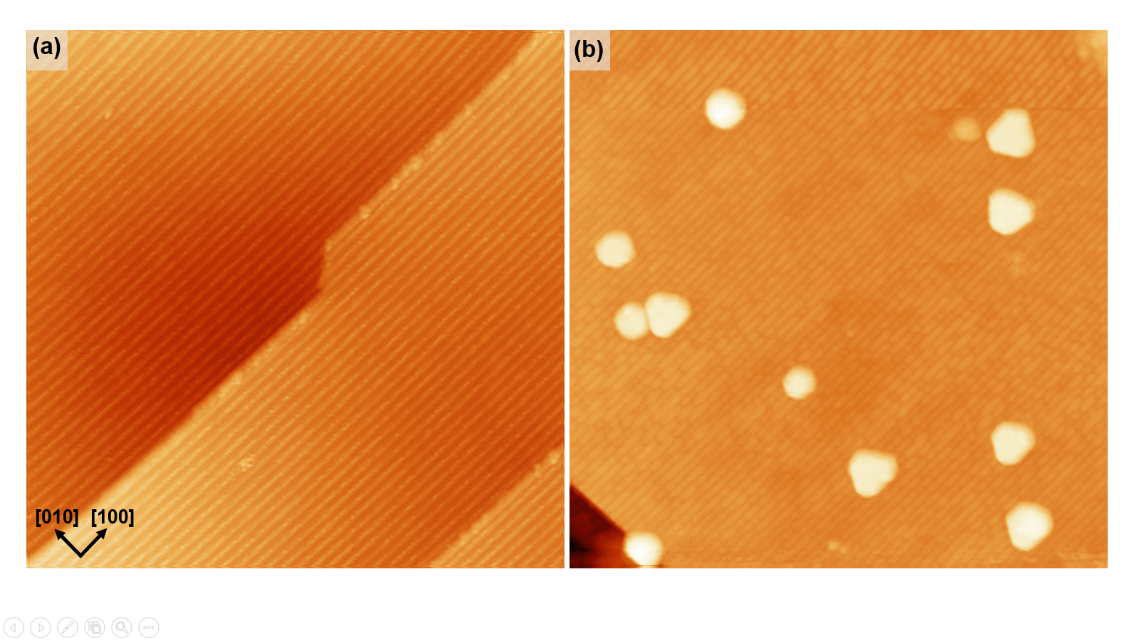
Figure 1: STM image of (a) anatase TiO2(001)-(1×4) surface (80×80 nm2, Vs = +1.61 V, It = 0.225 nA); (b)Pd nanocrystals grown on anatase TiO2(001) surface (100×100 nm2, Vs = +2.5 V, It = 0.8 nA).
Poster
Structure and Growth of Monatomic TM-Oxide Chains - Copper Against All Others
1Solid State Physics, Friedrich-Alexander University Erlangen-Nuremberg, Erlangen, Germany
2Applied Physics, Technical University Vienna, Austria
Annealing submonolayer deposits of 3d transition metals (TM) on Ir(100) in oxygen leads to a self-organised growth of TMO2 chains with monatomic metal core [1]. We have investigated the growth, geometrical structure and energetics of these systems by scanning tunneling microscopy, quantitative LEED-IV analyses and density functional theory.
In case of TM = Mn, Fe, Co and Ni the oxide chains grow from the very beginning in islands with 3×1 periodicity, which is the closest possible mutual chain distance. Eventually, at a coverage of 1/3 monolayer a homogeneous phase develops. Therefore, this phase has to be regarded as a 2-dimensional phase despite the quasi one-dimensional appearance of single chains: The monatomic metal core of the chains is found to be shifted by half a substrate unit vector against the substrate with every transition metal atom being fourfold coordinated to oxygen. Below every oxide chain the Ir row is missing so that the oxide chains resides well above this trough avoiding any direct binding of the TM core with the substrate.
In stark contrast, CuO2 is found to form (n×2) ordered phases with n=1/θCu (or c(8×2) in case of n=4), consisting of equally spaced chains according to the respective Cu coverage θCu.
The space between the oxide chains is filled by narrow stripes of oxygen atoms with a local structure very similar to that of the (2×1)-O phase of oxygen on plain Ir(100) [2]. Additionally, the local chain structure deviates substantially from the other TM chains: Though the Cu core is also shifted against the substrate rows, every Cu atom is now only twofold coordinated to oxygen. Further, the Cu core lies deep within the troughs of the substrate missing row reconstruction forming two more bonds towards Ir atoms of the second layer.
Accompanying DFT calculations closely reproduce the LEED bestfit structural parameters as well as the STM appearance for all systems. The structure of the copper chains is only by less than 0.1 eV more favourable than the alternative structure corresponding to all other TM oxide chains. Therefore, the structural switch is induced by a cooperation of various contributions.
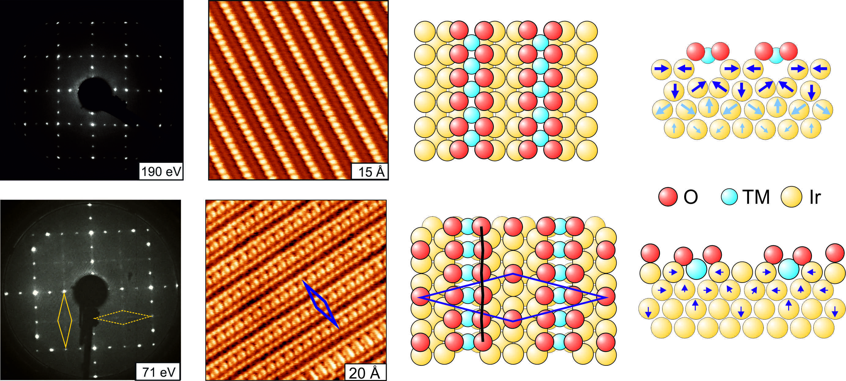
Figure 1: Appearance of the (3×1)-CoO2 (upper row) and c(8×2)-CuO2 (bottom row) phases in LEED and STM as well as the corresponding ball models in top and side view.
[1] P. Ferstl et al., Phys. Rev. Lett. 117, 046101 (2016)
[2] P. Ferstl et al., Phys. Rev. B 93, 235406 (2016)
Poster
Structural sensitivity of medium energy intensity data in a LEED analysis
1Solid State Physics, Friedrich-Alexander University Erlangen-Nuremberg, Germany
The crystallographic analysis of complex surface structures involves the quantitative determination of many structural parameters and therefore requires a large experimental data base. In low energy electron diffraction (LEED) intensities are taken as a function of energy, so called I(E)-spectra, within an energy range of typically 50-400 eV. A simple increase of the maximum energy would raise the amount of independent data quadratically.
In this study we demonstrate that such an extension of the energy range for a LEED analysis up to much higher energies (900 eV) does not necessarily lead to a loss of the surface sensitivity due to the increased penetration depth of the electrons. In contrast, the reduced relative scattering contribution of the surface layer is in most cases compensated by the increased structural resolution provided by the smaller electron wave length at higher energies. This holds for most scatterers except for light-weighted or heavily vibrating atoms. Moreover, the high energy data show as expected a much higher sensitivity to structural details within deeply buried layers.
The applicability of this approach is not only predicted by model calculations but also demonstrated experimentally for various structurally quite different systems. We compare the structural sensitivity of low and high energy data sets obtained for clean surfaces of a Rh(100) bulk crystal, a thick CoO(100) film, as well as different ordered phases of transition metal surface oxides on Ir(100). The extension of the energy range also improves the reliability of the LEED analysis and by that allows to determine structural parameters with a precision of one single picometer in favourite cases.
In turn, higher energy data are also more sensitive to the angle of incidence of the primary electron beam. This eventually demands for some corrections for the (slightly) convergent beam used in the experiment which are also introduced in this contribution.
Figure 1: R-Factor curves RP vs parameter variation for the Ir(100)-3×1-CoO3 phase. Green lines correspond to the LEED-fit within the full energy range 50-800 eV, red lines to the low energy (50-350 eV) and blue lines to the high energy regime (650-800 eV). The top row compares the relative sensitivity on the vertical position of surface and buried Ir atoms; the bottom row corresponds to surface cobalt and oxygen atoms. For Ir and Co the positional sensitivity is superior in the high energy range, only for the lighter oxygen atoms the situation is reversed.
Poster
The structure of the SnO2(110)-(4x1) reconstruction
1 Lund University, 22100 Lund, Sweden
2 Aarhus University, DK-80000 Aarhus C, Denmark
3 LUT School of Engineering Science, P.O. Box 20, FIN-53851 Lappeenranta, Finland
4 Diamond Light Source, Harwell Science and Innovation Campus, Didcot OX11 0DE, UK
5 University College London, London WC1H 0AJ, United Kingdom
6 The University of Manchester, Sackville Street, Manchester M13 9PL, UK
SnO2 is an important material for a number of applications such as gas sensors, catalysis and photo electronics [1], but a detailed understanding of some of the functions of the material is missing due to a lack of knowledge of the surface composition and the exact atomic arrangement. It is however known that a number of applications are based on the dual valency of Tin oxide, and the oxide prefers oxidation states of 2+ or 4+. The SnO2 crystallizes in the rutile phase, and the most stable termination is the (110) phase, having a bulk terminated surface structure similar to TiO2(110) and RuO2(110) [1]. Early surface studies suggested that an oxidized (110) surface could be reduced upon heating and forming a disordered (1x1) termination, and only by sputtering the surface before annealing results in a more well-ordered (4x1) reconstruction, suggesting oxygen depletion by preferential sputtering of oxygen atoms at the surface [2,3].
The surface structure of the SnO2(110)-(1x4) has been studied by several methods [4-7], and a model consisting of an in-plane oxygen vacancy structure [4,5] has been proposed, which was confirmed by Low Energy Electron Diffraction (LEED) [6] and Density Functional Theory (DFT) [7], the latter with slightly different relaxations compared to the former. Later, observations of 1Å deep antiphase domain boundaries by Scanning Tunneling Microscopy (STM) in the (4x1) structure could not be explained by the existing vacancy model. Instead, an overlayer was suggested, and a model based on Sn-O broken "chains" was proposed [8].
We have studied the SnO2(110)-(4x1) reconstruction by a combination of Surface X-Ray Diffraction (SXRD), X-Ray Absorption Spectroscopy (XAS), DFT, and quantitative LEED. The SXRD measurements implies a single quasi-hexagonal Sn overlayer on the SnO2(110) surface, and the models in ref [4-8] did not show a satisfying agreement with the experimental data. While the oxygen atoms are more difficult to observe in SXRD, XAS directly indicate the presence of 2+ Sn atoms in the structure, suggesting an oxygen depleted SnxOy overlayer. Using an evolutionary algorithm (EA) [9, 10] implemented in the Atomic Simulation Environment (ASE) [11] software, global minimum structures were found for different SnxOy compositions, and their stability at 1100K was investigated. A Sn6O6 overlayer was found to be more stable than the bulk termination and all other calculated structures. The theoretical structures were tested with the SXRD data, and the best theoretical model showed a good agreement. The model was also used to simulate existing STM images [8], displaying excellent agreement between data and theory.
[1] M. Batzill and U. Diebold, Prog. Surf. Sci 79, 47(2005).
[2] E. de Frésart, J. Darville and J.M. Gilles, Solid State Commun. 37, 13(1982).
[3] D.F. Cox, T.B. Fryberger and S. Semancik, Surf. Sci. 224, 121(1989).
[4] F.H. Jones, R. Dixon, J.S. Foord, R.G. Egdell and J.B. and Pethica, Surf. Sci. 376, 367(1997).
[5] M. Sinner-Hettenback et al., Surf. Sci. 447, 50(2001).
[6] A. Atrei, E. Zanazzi, U. Bardi and G. Rovida, Surf. Sci. 475, L223(2001).
[7] J. Oviedo and M.J. Gillan, Surf. Sci. 513, 26(2002).
[8] M. Batzill, K. Katsiev, and U. Diebold, Surf. Sci. 529, 295(2003).
[9] L.B. Vilhelmsen and B. Hammer, Phys. Rev. Lett. 108, 126101(2012).
[10] L.B. Vilhelmsen and B. Hammer, J. Chem. Phys. 141, 044711(2014).
[11] S.R. Bahn and K.W. Jacobsen, Comput. Sci. Eng. 4, 56(2002).
Poster
Coherent optical and acoustic phonons at buried GaP/Si interfaces
1National Institute for Materials Science, Tsukuba, 3050047 Japan
2Department of Physics, University of Florida, Gainesville, FL 32611 USA
3Material Science Center and Faculty of Physics, Philipps University Marburg, 35032 Marburg, Germany
4Department of Physics and Astronomy, University of Pittsburgh, Pittsburgh, PA 15260 USA
Photoexcitation of a solid with a femtosecond laser pulse can lead to the generation of coherent phonons. Coherent optical phonons are non-propagating lattice oscillations with zero wavevectors and discrete THz frequencies, whereas coherent acoustic phonons, by contrast, are ultrasonic strain pulses that can have a broad spectrum from GHz up to a few THz frequencies and wide range of wavevectors. Here we present our combined experimental-theoretical studies on both coherent phonons generated at the lattice-matched GaP/Si interfaces, whose GaP overlayers are grown by MOVPE on n-type Si(001) substrates and characterized by STEM [1]. We perform pump-probe reflectivity measurements using laser pulses of 400-nm wavelength and 10-fs duration as a light source. On the sub-picosecond time scale, the reflectivity changes of the GaP/Si samples, shown for a 56-nm thick GaP layer on Si in Fig. 1a, are modulated at very fast (~10 THz) oscillations, which is comprised of the longitudinal optical (LO) phonons of GaP and Si. We find the amplitude of the LO phonon of GaP to depend critically on the growth condition of the GaP overlayers. Since the coherent LO phonons of polar semiconductors are predominantly generated by the sudden screening of the built-in surface field, we can estimate the band bending on both sides of the GaP/Si interfaces based on the LO phonon amplitude with help of simple theoretical modeling [2]. On the longer time scale, the reflectivity change is modified at slower (~0.1 THz) oscillations, as shown in Fig. 1b. The slow modulations are periodic for GaP and Si, and their frequencies agree with those of the "Brillouin oscillation", i.e., the interference between the reflections from the surface and a moving acoustic pulse [3]. The GaP/Si samples also show similar slow modulations, but with complicated phase jumps as well as a sharp spike (indicated by an arrow in Fig. 1b). The reflectivity spike appears at a time required for the longitudinal acoustic (LA) phonons to traverse the GaP layer, and is attributed to the acoustic pulse generated at the GaP/Si interface and detected at the GaP/air surface. The extremely narrow temporal width, ~0.5 ps, corresponds to a spatial extent of ~3 nm or 10 Ga-P bilayers. The generation of the acoustic pulse can be explained in terms of the ultrafast charge separation at the GaP/Si interface, leading to the effective deformation potential coupling constant that is different from intrinsic values in GaP and Si crystals.
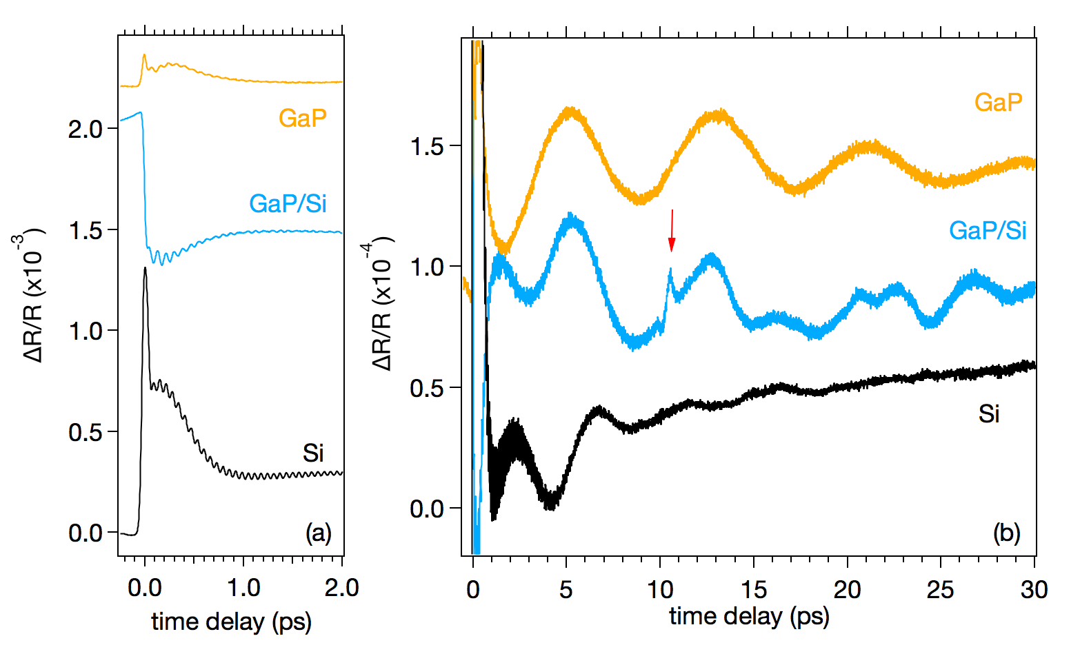
Figure 1: Transient reflectivity change of a 56-nm thick GaP layer grown on Si(001), together with those of (001)-oriented GaP and Si. Panels (a) and (b) show identical data with different expansions.
[1] A. Beyer, A. Stegmüller, J.O. Oelerich, K. Jandieri, K. Werner, G. Mette, W. Stolz, S.D. Baranovskii, R. Tonner, and K. Volz, Chem. Mater. 28, 3265 (2016).
[2] K. Ishioka, K. Brixius, A. Beyer, A. Rustagi, C.J. Stanton, W. Stolz, K. Volz, U. Höfer, and H. Petek, Appl. Phys. Lett. 108, 051607 (2016).
[3] K. Ishioka, A. Rustagi, U. Höfer, H. Petek and C.J. Stanton, Phys. Rev. B 95, 035205 (2017).
Poster
Structure Determination Considering Surface Dynamics: The O/Rh(100) System
1Solid State Physics, Friedrich-Alexander University Erlangen-Nuremberg, Erlangen, Germany
In this study we combine quantitative LEED-IV, STM and DFT calculations to reinvestigate the oxygen phases on Rh(100) up to a coverage of 0.67 ML. In this regime three distinct phases exist: A (2x2)-O [1], a (2x2)-2O [2] and a (3x1)-2O structure [3]. Their appearance in LEED and room temperature STM is displayed in Fig.1.
Regarding the (3×1)-2O phase our LEED analysis validates the structural model proposed by Gustafson et al. [3] with a Pendry R-factor RP = 0.096. The resulting structural parameters coincide almost quantitatively to those obtained for the Pt25Rh75(100)-(3×1)-2O structure [4].
For the (2×2)-O phase our LEED re-analysis (RP = 0.072) corroborates the hollow site adsorption revealed by the early analysis of Oed et al. [1] and refines their structural model by the determination of 13 additional parameters. This finding, however, contrasts to the appearance in room temperature STM, where non-primitive (2×2), (2×1) and (1×1) areas are imaged (cf. Fig.1). We interpret these features as a time average over rapidly fluctuating light domain walls which is corroborated by small diffusion barriers (190 meV) as obtained by DFT.
In case of the (2×2)-2O structure our LEED analysis confirms the model of a clockwise-/ anticlockwise reconstruction of the substrate. However, contrary to the analysis of Baraldi et al. [2], our best-fit structure (RP = 0.098) correctly accounts for all symmetry elements observed in experiment. This is achieved by introducing a 50 : 50 occupation of neighboring quasi-threefold oxygen adsorption sites. As proposed by Alfè et al. [4] and confirmed by our DFT calculations these sites are separated by a barrier as low as 24 meV.
Thus, every single oxygen atom fluctuates with close to phonon frequency preventing the substrate from a complete, symmetry-breaking local relaxation. Of course, STM can only see the mean positions of the hopping atoms and therefore pretends a simple c(2×2) configuration.
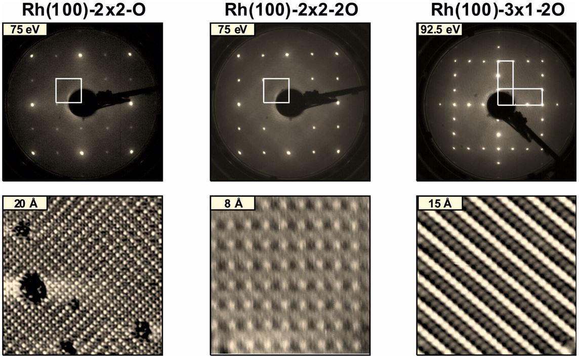
Figure 1: Overview of all investigated oxygen adsorption phases on Rh(100). Top row: LEED pictures. Bottom row: Corresponding atomically resolved room-temperature STM images.
[1] W. Oed et al., Surf. Sci. 207, 55 (1988)
[2] A. Baraldi et al., PRL 82, 4874 (1999)
[3] J. Gustafson et al., JPCM 24, 225006 (2012)
[4] M. Sporn et al., Surf. Sci. 416, 384 (1998)
[5] D. Alfè et al., Surf. Sci. 410, 151 (1998)
Poster
Robustness of topological surface states against magnetic perturbations
1Instituto de Nanociencia de Aragón (INA) & Laboratorio de Microscopias Avanzadas (LMA), University of Zaragoza, 50018 Zaragoza, Spain
2Department of Condensed Matter Physics, University of Zaragoza, 50009, Zaragoza, Spain
3Fundación Instituto de Nanociencia de Aragón (FINA), 50018, Zaragoza, Spain
4Donostia International Physics Center (DIPC), E-20018 San Sebastián, Spain
5Ames Laboratory, U.S. Dept. of Energy, Ames, IA 50011, USA 4
6Department of Materials Sciences & Engineering, Iowa State University, Ames, IA 50011, USA
7IKERBASQUE, Basque Foundation for Science, E-48011 Bilbao, Spain
Topological insulators (TIs) have attracted a lot of interest in the last few years due to the unique properties of their surface states, which are protected by time-reversal symmetry (TRS). Electrons in these topological surface states can not be backscattered, making TIs promising candidates for their application in high performance electronics and spintronics. For potential spintronic devices, however, it is necessary to establish contacts between the TI and other magnetic materials. This could lead to a breaking of the time-reversal symmetry and, consequently, to a destruction of the topological surface state [1,2].
In this combined experimental and theoretical study we investigate the influence of magnetic adatoms, namely Co, on the structural and electronic properties as well as on the topological surface states of Bi2Te3 and Bi2(Seδ,Te1-δ)3 (BST). Scanning tunneling microscope (STM) measurements indicate that, on the BST surface, the Co adatoms move away from the high symmetry points of the surface unit cell. Our density functional theory (DFT) calculations of the relaxed surface structures strongly support the results of these measurements. We also find, from our first-principles calculations, that the direction of the magnetic moment of the adatoms depends on the adsorption site and local environment. Thus, since an in-plane magnetic moment might mask TRS breaking [3], a 3 Tesla magnetic field is applied in the STM experiments. According to our DFT predicted low magnetic anisotropy energies this magnetic field guarantees a sizable out-of-plane magnetic moment. Our experiments show that, upon Co adsorption, the TRS is preserved for the BST surface while it is destroyed for the Bi2Te3. The preservation of TRS in BST is attributed to a lack of hybridization between the Co states and the topological surface state, for which we found experimental evidence in the absence of Co states within the bulk bandgap [4].
[1] P. Sessi et al., Nat. Commun. 5, 5349 (2014)
[2] Y. L. Chen et al., Science 329 (5992), 659-662 (2010)
[3] M. Ye et al., Phys. Rev. B 85, 205317 (2012)
[4] M. C. Martinez-Velarte, B. Kretz et al., Under review.
Poster
Understanding the Geometric Structure of a Superconductor with a Strain Induced High Tc
1Diamond Light Source, Didcot, UK
2Technical University of Munich, Munich, Germany
3Fudan University, Shanghai, China
Utilising high Tc superconductors technologically has been beset by a myriad of technical issues. The standard bearer of high Tc superconductors, the cuprates, do not exhibit the performance known from the bulk as the monolayer limit is approached[1]. However FeSe thin films, grown on SrTiO3 (STO) substrates show a dramatic increase in Tc, compared to their bulk value (8 K). In fact, the highest Tc (over 60K) have been observed for FeSe monolayers[2]. This temperature exceeds all Tc of the known bulk iron-based superconductors, while still maintaining a comparatively simple composition. It is likely that the interaction between the STO and the FeSe is playing a significant role in this dramatic increase in Tc, thus gaining high precision geometric information of the adsorption structure of the FeSe on STO is of the utmost importance. Without such information, theoretical understanding of this phenomenon will remain elusive. To this end we have pursued a joint X-ray standing wave (XSW) and energy scanned photoelectron diffraction (PhD) study into the geometry of this system.
XSW triangulation has determined that the Fe atoms sit in a site above the bulk oxygen atoms in the Ti planes. However, due to a lack of chemical shift in the Se 3p XP spectra, it has not been possible to determine the Se absorption site of the two non-identical Se atoms, see figure 1 a). Therefore Se 1s and Fe 1s PhD measurements, see figure 1 b), were pursued in order to precisely illuminate the fine structure of the FeSe, and the interaction between the FeSe and the STO.
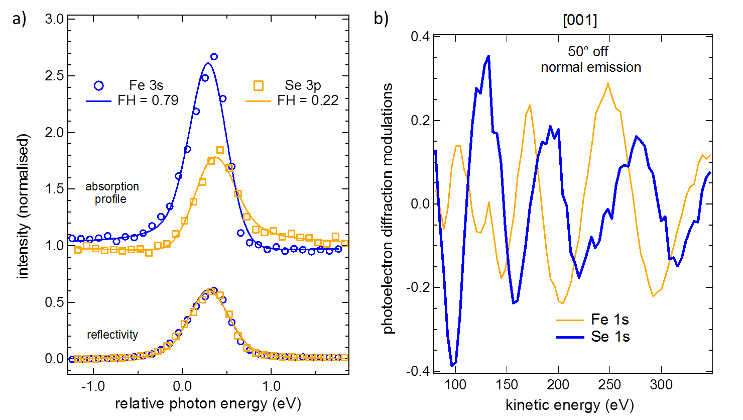
Figure 1: ) Comparison of the Fe 3s and Se 3p XSW from FeSe on SrTiO3. Note that the Se 3p XSW displays a significantly lower coherent fraction, FH, indicative of two distinct adsorption sites. b) Comparison of the Fe 1s and Se 1s PhD spectra indicating dramatically different periodicity, but comparable amplitude modulations.
[1] G. Logvenov et al., Science 326, 699 (2009)
[2] J.-F. Ge et al., Nat. Mater. 14, 285 (2015)
[3] S.Y. Tan et al., Nat. Mater. 12, 605 (2013)
Poster
Initial stages of mixed nickel-iron oxides growth on Ru(0001)
1Instituto de Química Física "Rocasolano", Madrid, 28006, Spain
2Dpto. De Física de Materiales, Universidad Complutense de Madrid, Madrid 28040, Spain
3Unidad Asociada UCM-IQFR(CSIC), Madrid 28006, Spain
4Dpto. De Física Aplicada, Universidad Autónoma de Madrid, Madrid 28049, Spain
5Instituto de Cerámica y Vidrio (CSIC), Madrid 28049, Spain
6Alba Synchrotron Light Facility, CELLS, Barcelona E-08290, Spain
Transition metal oxides (TMO) are promising candidate materials for future spintronic devices. Their properties arise from the interactions between transition metal and oxygen ions in a given structure which are very sensitive to different bond length and angles, as well as to their particular cationic distribution. Among them, the spinel family comprises a large number of compounds. Spinels have an fcc anion lattice with cations occupying tetrahedral and octahedral sites. Spinels can be half-metallic (like Fe3O4[1]), ferrimagnetic insulators, superconductors (LiTi2O4[2]) or heavy fermion materials. However, their properties in thin film growth, as necessary for devices, are often disappointing, dictated by the defect density.
Here we demonstrate a method for preparing high quality ultrathin TMO films on a metallic substrate. Mixed nickel-iron oxides have been grown on Ru(0001) by oxygen-assisted molecular beam epitaxy at elevated temperatures (800 - 900K). The nucleation and growth process are observed in situ by means of Low Energy Electron Microscopy (LEEM). A comprehensive characterization is performed combining LEEM for structural characterization and PEEM (PhotoEmission Electron Microscopy) with synchrotron radiation for chemical and magnetic analysis via X-ray Absorption Spectroscopy and X-ray Magnetic Circular Dichroism (XAS-PEEM and XMCD-PEEM, respectively). The latter permits imaging the element specific magnetic domain structure.
We will show that the growth by oxygen-assisted molecular beam epitaxy takes place in two stages. First, monoxide islands nucleate and grow until they completely cover the substrate surface. Later three-dimensional islands of spinel phase grow on top of the monoxide layer. Only the spinel islands show magnetic contrast, with the same domains being observed in the Fe and Ni XMCD images.
[1] K. Siratori et al., J. Phys. Soc. Jpn. 53, 312 (1984)
[2] D. C. Johnston et al., Mater. Res. Bull. 8, 777 (1973)
Poster
Electronic Structure Characterization of atomically-precise Chiral Graphene Nanoribbons on gold surfaces
1CIC nanoGUNE, 20018 Donostia-San Sebastián, Spain
2Donostia International Physics Center, 20018 Donostia-San Sebastián, Spain
3Centro de Física de Materiales (CSIC/UPV-EHU) - Materials Physics Center, 20018 Donostia -San Sebastián, Spain
4Ikerbasque, Basque Foundation for Science, 48013 Bilbao, Spain
5Centro de Investigación en Química Biolóxica e Materiales Moleculares (CIQUS) and Departamento de Química Orgánica, 15782 Universidad de Santiago de Compostela, Spain
Graphene nanoribbons (GNRs) are narrow stripes of graphene that have attracted great attention because of their interest for both fundamental physics and promising applications. While sharing many of the appealing properties of their predecessor material graphene, such as high mobility charge-carriers and high specific surface area, they overcome some of its limitations as is the lack of a band gap. These nanostructures can display different edge orientations with respect to graphene´s lattice vectors that largely determine their main properties. Therefore three types of ribbons can be synthesized: armchair, zigzag or chiral GNRs, the latter ones presenting a periodic combination of both armchair- and zigzag-like segments. A recently established bottom-up synthesis method based on the use of molecular precursors as building blocks allows for the synthesis of these three types of GNRs with atomic precision [1]. However, the limited experimental results on these structures are mostly focused on the electronic structure of armchair and, to a lesser extent, on zigzag GNRs, thus letting chiral GNRs (cGNRs) hardly explored. The growth of these ribbons on different noble metals was recently reported [2], hence we focus on the electronic structure of these nanomaterials.
Here, using the same molecular precursor-based methodology, we report on the electronic structure of (3,1)-cGNRs on Au(111) by Scanning Tunneling Spectroscopy (STS). Moreover, the use of Au(322) vicinal substrate as template promotes the aligned growth of these ribbons along the terrace length thus enabling us to characterize the valence band by means of ARPES. Our results reveal a semiconducting bandgap on these chiral nanoribbons therefore confirming its potential applications for nanoelectronics.
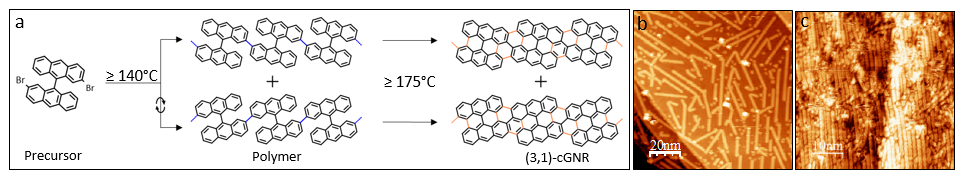
Figure 1: (a) Synthetic scheme and topographic images of (3,1)-cGNR on (b) Au (111) and (c) Au(322) surfaces.
[1] J. Cai et al., Nature 466,470-473 (2010)
[2] D.G. de Oteyza et al., ACS Nano 10, 9000-9008 (2016)
Poster
Surface spectroscopy and spin filtering of DPEDA chiral molecular film
1Instituto Madrileño de Estudios Avanzados en Nanociencia (IMDEA), 28049 Madrid (Spain)
2Dpto. Física de la Materia Condensada (UAM), 28049-Madrid (Spain)
3Polish Academy of Sciences, Al Lotnikow 32/46, PL-02-668 Warsaw (Poland)
4ALBA-CELLS Synchrotron, Cerdañola del Vallés, 08290 Barcelona (Spain)
5Dpt. of Physics Uppsala Univeristy, Box 516, SE-7120 Uppsala (Sweden)
Chiral structures, and in particular chiral molecules, are fascinating objects in many areas: in Physics the relationship between chirality and magnetism has puzzled researchers since the 19th century, and only in the 21th century we have learn to make use of this relationship, for example using the ability of chiral layers to scatter electrons differently depending on their spin [1]. From this technological point of view, chiral surfaces open the door to use in 2D devices different properties like chiral selectivity, enantiospecific chemical reactions [2] or the possibility to use these materials as, for instance, spin filters [3].
Thin films of pure enantiomeric diphenil ethane diamine (DPEDA) and diphenyl ethane diol (DPED) have been grown in UHV on Cu(001) and on Co/Cu(100) surface. We have used surface sensitive spectrocopies based on synchrotron techniques (XAS, XPS, spin polarized UPS, XPEEM) to study the influence of the chirality on the magnetism, demonstrating with X-ray circular natural dichroism (XNCD) measured at the C K-edge the preservation of the chiral character of these molecular thin films in the electronic structure. The effect of this chiral molecular film adsorbed on ferromagnetic cobalt has been measured though XMCD at the Co L-edges, showing a change in the magnetic moment in the cobalt atoms at the surface, with the implication of a charge transfer with spin polarization.
More indeed, in electron currents photoemitted from molecular films of DPED and DPEDA adsorbed on Co/Cu(100) surfaces we have observed macroscopic spin polarizations, showing that chiral molecules in a non-spiral geometry can filter spin electrons. These measurements also show that the different enantiomers of the same molecule can produce spin polarizations oriented along different directions in space [4].
[1] K. Ray et al., Science 283, 814 (1999).
[2] A. Gellman et al., J. Am. Chem. Soc. 135, 19208 (2013).
[3] B. Göhler et al., Science 331, 894 (2011).
[4] M. A. Niño et al., Adv. Mat. 26, 7474 (2014).
Poster
Decoding crystallographic domains of molecular systems by cantilever torsion imaging
1Insitut de Ciència de Materials de Barcelona (ICMAB-CSIC) Campus de la UAB, Cerdanyola del Vallès 08190 Barcelona, Spain
2 Otto Schott Institute of Materials Research, Friedrich Schiller University Jena, 07743 Jena, Germany
3Catalan Institute of Nanotecnology (ICN), UAB Campus, E-08193 Bellaterra, Spain
4Instituto de Ciencia de Materiales de Madrid, CSIC Madrid, 28049, Spain
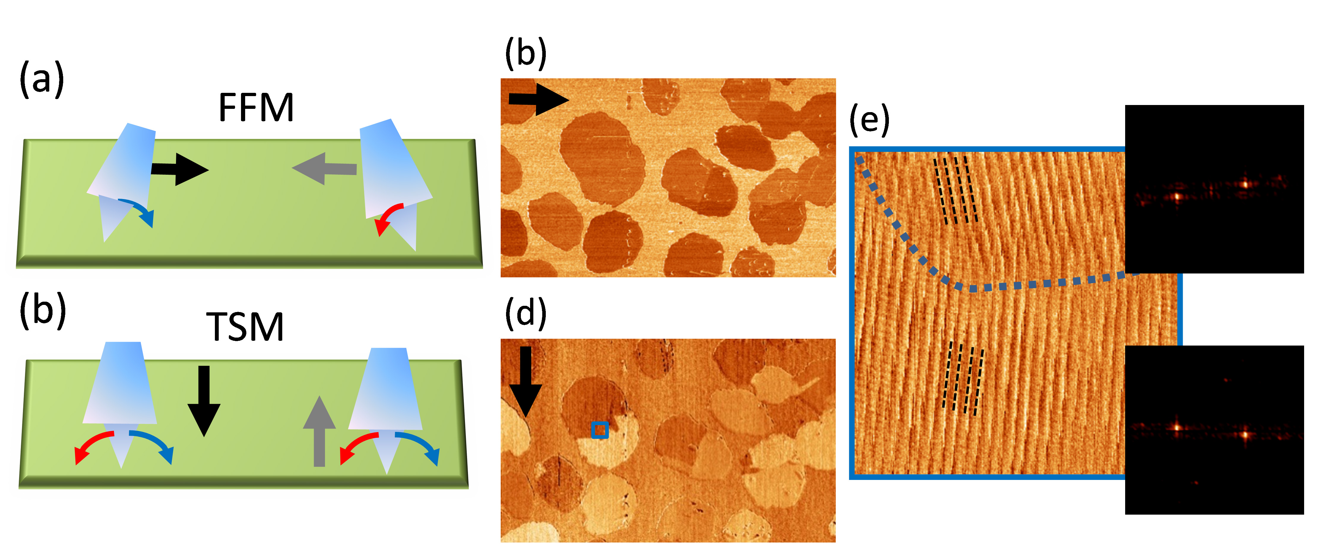
From the physical point of view, the tribological response, in particular frictional properties, of organic surfaces is an obvious subject of interest by itself. As a powerful tool to understand different dissipation mechanisms at surfaces, we commonly employ the scanning force microscope by measuring the lateral force perpendicular to the scan direction (also known as friction force microscopy, FFM). As for inorganic materials, FFM helps visualizing regions of different chemical nature. However, more subtle surface characteristics influence the frictional properties of molecular systems and well-designed and sensitive FFM measurements permit obtaining detailed structural details as molecular order (stick-slip) as well as molecular tilt angles and/or tilt angle azimuths. This is the case of observing friction anisotropy or friction asymmetry. The term anisotropy refers to the variation of friction with the relative orientation angle between sliding surfaces and is commonly correlated with surface crystallographic orientations, while asymmetry refers to a change in friction when the sliding direction is changed by 180°. FFM has been successfully employed in organic self-assembled monolayers (SAMs) not only to discriminate between ordered configurations presenting different friction coefficients or different packing, but also to decipher between equivalent structural domains as well as to identify highly dissipative transient molecular configurations during phase transitions. Outstandingly, crystallographic aspects including "stick-slip" can also be extracted from the torsion of the cantilever during scanning along its axis in the so-called transverse shear microscopy (TSM).
[1] E. Barrena, C. Ocal, M. Salmeron. Journal of Chemical Physics 113(6), 2413- 2418 (2000)
[2] C. Munuera, C. Ocal. Journal Chemical Physics 124(19), 206102-1-5 (2006)
[3] C. Munuera, E. Barrena, C. Ocal. Journal of Physical Chemistry A 111(49), 12721-12726 (2007)
[4] M. Paradinas, L. Garzón, F. Sánchez, R. Bachelet, D.B. Amabilino, J. Fontcuberta, C. Ocal. Phys. Chem. Chem. Phys. 12, 4452-4458 (2010)
[5] J.J. Segura, A. Verdaguer, L. Garzón, E. Barrena, C. Ocal, J. Fraxedas. J. Chem. Phys. 134(13), 124705-1-9 (2011)
[6] M. Paradinas, C. Munuera, Ch. Silien, M. Buck, C. Ocal, Phys. Chem. Chem. Phys. 115(4)1, 1302-1309 (2013)
[7] A. Pérez, E. Barrena, A. Fernández, E. Gnecco, C. Ocal (2017 submitted)
Poster
Structure and electronic states of vicinal noble metal surfaces with densely kinked steps
1Donostia International Physics Center DIPC, San Sebastián, Spain
2Centro de Física de Materiales, CFM-CSIC, San Sebastián, Spain
3Instituto de Ciencia de Materiales de Aragón (ICMA), Universidad de Zaragoza, Spain
4Department of Physics, University of Maryland, College-Park, Maryland, USA
5Departamento de Física Aplicada I, Universidad del País Vasco, San Sebastián, Spain
The thermal excitation of step-edge atoms into "kinks" (e-εkT) is the essence of the step dynamics on a crystal surface. At a vicinal surface with high step densities, kinks also influence the equilibrium shape at finite temperature. At T=0, the density of kinks strongly depends on the in-plane orientation of the surface. At fcc -(111) vicinal planes close-packed step-edges (A-type and B-type) run parallel to equivalent [1-10] directions. As shown in Fig. 1a, steps oriented along the [11-2] direction exhibit a "100% kinked" step-edge (K-type), where out-protruding step-edge atoms have no direct nearest-neighbors parallel to the step. Remarkably, as sketched in the same Fig. 1a, in such K-steps thermal excitations have zero energy cost ε=0, allowing meandering and roughening of steps without energy penalty. Our objective is to investigate, theoretically and experimentally, the impact of this property in step dynamics, equilibrium shape, growth, and electronic states of K-stepped surfaces.
First experiments have been performed using a Ag single crystal curved around the (654) direction, which allows one to probe with STM and Angle Resolved Photoemission (ARPES) all K-type vicinal surfaces from the (111) plane up to α=18°. In Fig. 1b we show characteristic STM images and terrace-width distribution histograms for α=2.26° and α=12.03°. A remarkably neat transformation is observed from low to high step-densities, suggesting a dramatic transition in step interactions, from purely entropic, at low step-densities, to strongly elastic, at high step-densities. In Fig. 1c we show the energy shift ΔE of the Shockley band measured with Angle Resolved Photoemission across the curved sample. Large ΔE values are found compared to close-packed steps, indicating strong repulsive scattering due to a larger electric dipole at K-type steps. The connection of these STM and ARPES results with the particular step energetics and dynamics of K-type vicinal surfaces will be discussed.
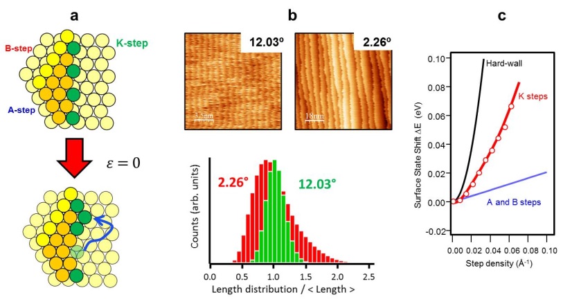
Figure 1: (a) Schematic description of atomic K-steps and the thermal excitation of step-edge atoms, with zero energy cost. (b) STM images (top) and terrace width distribution analysis (bottom) of two K-stepped surfaces. Experiments are performed on a curved Ag(654) crystal. (c) Surface state shift as a function of the step density, measured by ARPES on the Ag(654) curved crystal.
Poster
Non-Covalent Dimerization after Enediyne Cyclization on Au(111)
1Donostia International Physics Center, E-20018 San Sebastián, Spain
2Ikerbasque, Basque Foundation for Science, E-48011 Bilbao, Spain
3Centro de Física de Materiales, E-20018 San Sebastián, Spain
4Nano-Bio Spectroscopy Group and ETSF, Universidad del País Vasco, CFM CSIC-UPV/EHU-MPC, 20018 San Sebastián
5Department of Physics, University of California, Berkeley, CA 94720, USA
6Department of Chemistry, University of California, Berkeley, CA 94720, USA
7Materials Sciences Division, Lawrence Berkeley National Laboratory, Berkeley, CA 94720, USA
8Kavli Energy NanoSciences Institute at the University of California Berkeley and the Lawrence Berkeley National Laboratory, Berkeley, CA 94720, USA
9Max Planck Institute for the Structure and Dynamics of Matter, 22761 Hamburg, Germany
10Center for Free-electron Laser Science (CFEL), Luruper Chaussee 149, 22761 Hamburg, Germany
We investigate the thermally-induced cyclization of 1,2-bis(2-phenylethynyl)benzene on Au(111) using scanning tunneling microscopy and computer simulations. Cyclization of sterically hindered enediynes is known to proceed via two competing mechanisms in solution: a classic C1-C6 or a C1-C5 cyclization pathway [1]. On Au(111) we find that the C1-C5 cyclization is suppressed and that the C1-C6 cyclization yields a highly strained bicyclic olefin whose surface chemistry was hitherto unknown. The C1-C6 product self-assembles into discrete non-covalently bound dimers on the surface (Fig. 1). The reaction mechanism and driving forces behind non-covalent association are discussed in light of density functional theory calculations [2].
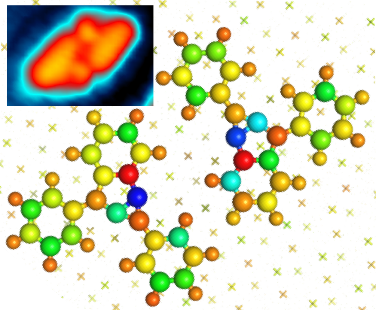
Figure 1: Scanning tunneling microscopy image of the dimer of cyclized products (inset) and the associated calculations on Bader charge distribution, evidencing the strongly polarized bonds responsible for the attractive dipole-dipole interaction.
[1] D.G. de Oteyza, in On-surface Synthesis ed. by A. Gourdon (Springer, 2016), p.85-99.
[2] D.G. de Oteyza et al., J. Am. Chem. Soc. 138, 10963 (2016).
Poster
Hierarchical chirality transfer during (S,S) and (R,R) DPEDA growth on Cu(100)
1Institut de Ciència de Materials de Barcelona (ICMAB-CSIC), Bellaterra 08193, Spain
2Dpto. Física de la Materia Condensada (UAM), Cantoblanco, 28049-Madrid, Spain
Obtaining spatially uniform chiral thin films with atomic-scale control of their handedness is a powerful way for developing nano-devices with novel chiral properties. In this sense, it is known that chirality on solid surfaces may exist at different levels of molecular assembly, from individual adsorbed species to 1D molecular chains or 2D molecular clusters and supramolecular patterns [1-4]. A chiral molecule is necessarily chiral upon adsorption and generally assembles in homochiral ordered 2D structures originated from the asymmetry of the molecule. Therefore, deposition of the opposite enantiomer will generate the mirror image systems.
In order to explore the origin of chiral transfer and amplification involved in the 3D assembling process, we investigate the self-assembly of two enantiomers of the Diphenylethylenediamine (DPEDA) molecule deposited from the vapor phase on Cu(100) under ultra-high-vacuum (UHV) and room temperature conditions. DPEDA possesses two chiral centres located at the two carbon atoms of the ethylene chain and presents two chiral enantiomers which are designated according to their conformation and optical activity as (R,R)-(+) and (S,S)-(-). The structure at the molecular level has been determined for different surface coverages by in-situ STM/FM-AFM. We show that the chirality of the DPEDA enantiomers is transferred at different levels of the molecular organization. Below the monolayer completion, each enantiomer arranges in two-dimensional (2D) domains of a supramolecular square lattice aligned with the principal crystallographic directions of the substrate (A-SQ). The intrinsic chirality of the molecule is only manifested within the unit cell (lack of mirror-symmetry). For increasing coverage, this A-SQ structure coexists with 2D domains of a square lattice (SQ) rotated ≈+11° or ≈-11° (for R,R or S,S, respectively) with respect to the principal direction of the Cu(100) substrate, as corresponds to enantiomeric mirror-like organization (Figure 1a). The 3D growth only occurs on top of the A-SQ structure and exhibits a clear chiral organization with an oblique unit cell. Interestingly, the chiral supramolecular order is unambiguously reflected in the chiral helicity observed for each enantiomer (Figure 1b and 1c).
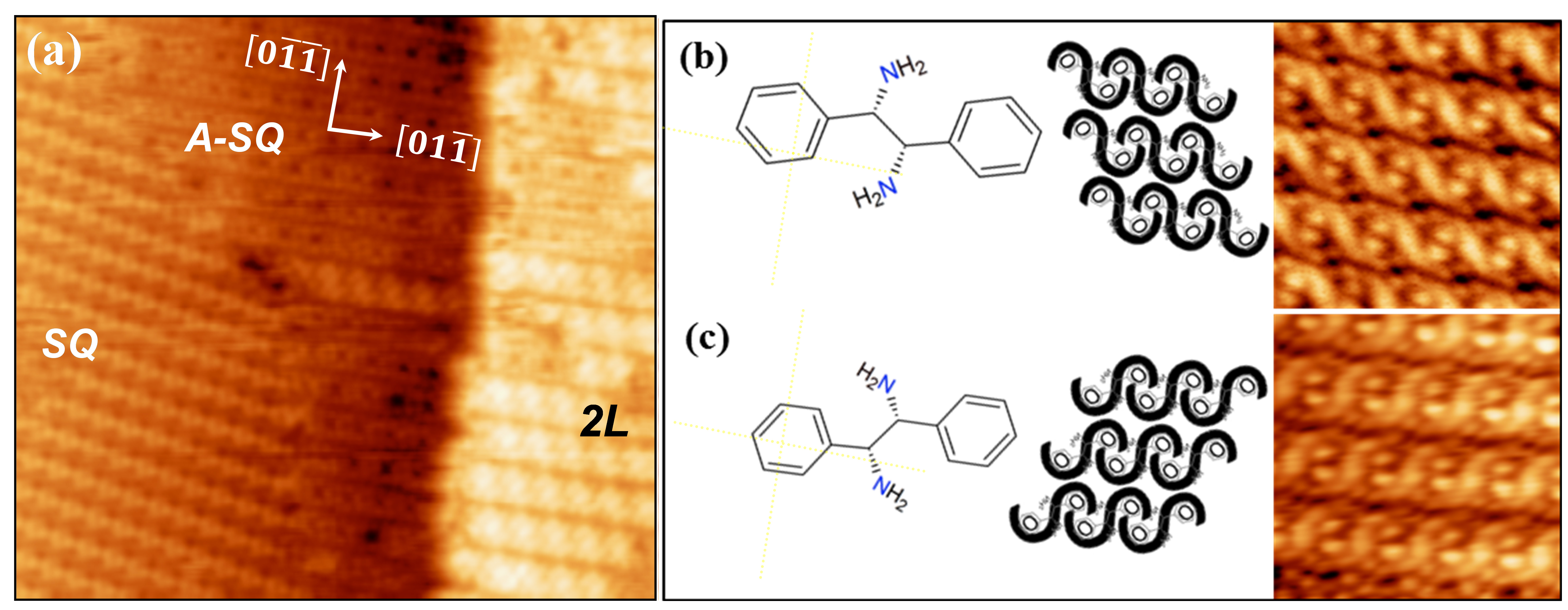
Figure 1: (a) STM image (30nm × 29nm) of (S,S)-DPEDA deposited on Cu(100) at room temperature. V = + 2V, I = 200pA. A second layer (2L) grows on top of a first layer in which domains of two square lattice structures (A-SQ and SQ) are seen. (b) and (c) magnification of the 2L structure (7nm × 7nm) for (S,S)-DPEDA and (R,R)-DPEDA.
[1] Barlow S. M. and Raval R., Surf. Sci. Rep. 50, 201-341 (2003).
[2] Raval R., Curr. Opin. Solid State Mater. Sci. 7, 67-74 (2003).
[3] Messina P., Dmitriev A. and Lin N., et al., J. Am. Chem. Soc. 124, 14000-1 (2002).
[4] Ting Chen, et al., Natl. Sci. Rev. 2, 205-216 (2015).
Poster
Structure of the SnO2 (110)-(4×1) with LEED I(E)
1 LUT School of Engineering Science, Lappeenranta, Finland
2 Division of Synchrotron Radiation Research, Lund University, Sweden
3 Interdisciplinary Nanoscience Center (iNANO) and Department of Physics and Astronomy, Aarhus University, Denmark
4 Diamond Light Source, Harwell Science and Innovation Campus, UK
5 Department of Chemistry and London Centre for Nanotechnology, University College London, UK
6 Corrosion and Protection Centre, School of Materials, The University of Manchester, UK
Tin dioxide (SnO2) is widely used as the active component of solid state gas sensors [1], and also has application in heterogeneous catalysis [2]. The basis for these applications is the reducibility of the oxide. The changes in conductivity of this n-type semiconductor resulting from surface processes are the basis for the material's gas-sensing characteristics. Because of this, it has long been a goal of fundamental research to characterize the structural, physical and chemical properties of SnO2 surfaces.
This work presents a quantitative low energy electron diffraction (LEED) analysis for the (4×1) reconstruction of SnO2 surface. A set of I(E) data for 15 inequivalent beams were collected with cumulative energy range of 1800 eV. The theoretical LEED intensities were fitted by using SATLEED program package [3]. The atomic coordinates for the Sn6O6 structure from a DFT calculation, scaled to the experimental lattice parameter of SnO2, were used as initial coordinates. The best fit structure, which differs from the DFT result by only a small (<0.1 Å) inward relaxation of the 6 Sn atoms, gives a Pendry reliability factor (RP ) [4] of 0.16, indicating that the model describes the experimental data well.
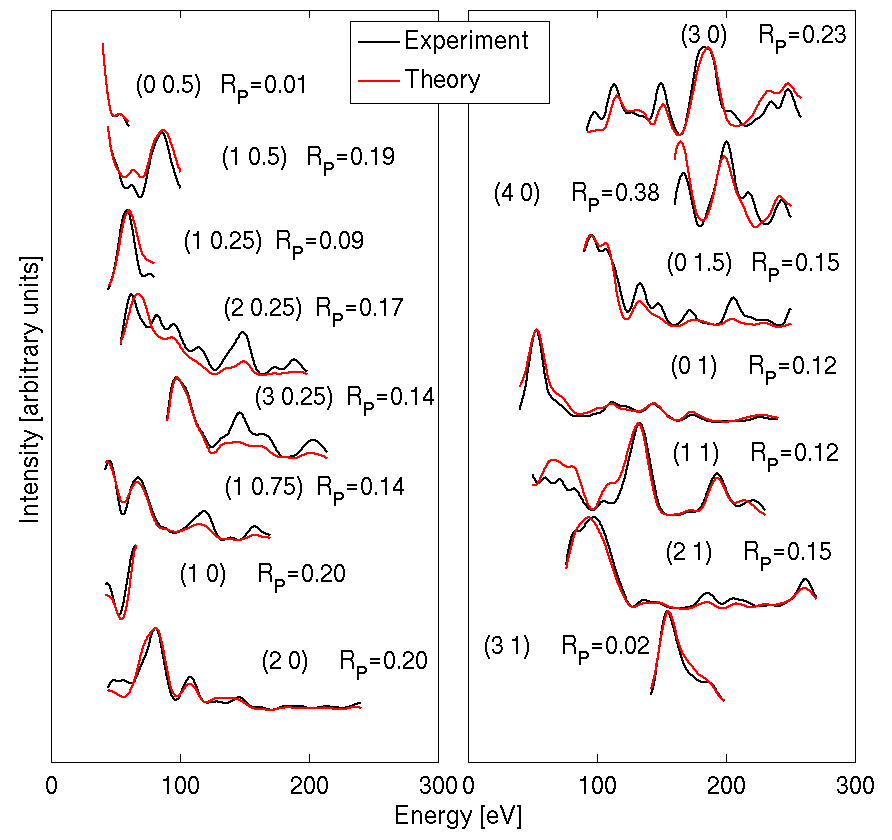
Figure 1: LEED I(V) measurements for SnO2(110)-(4×1). The cumulative RP was 0.16 .
[1] M. Batzill and U. Diebold, Phys. Chem. Chem. Phys. 9, 2307(2007).
[2] M. Batzill and U. Diebold, Prog. Surf. Sci. 79, 47(2005).
[3] A. Barbieri and M.A. Van Hove, private comm. (http://www.icts.hkbu.edu.hk/vanhove/).
[4] J.B. Pendry, J. Phys. C: Solid State Phys. 13, 937(1980).
Poster
Interplay between metal-organic interface state and donor-acceptor interface mediated charge separation on PTCDA/TiOPc/Ag(111)
1 Centro de Física de Materiales (CSIC), San Sebastián, Spain
2 Fachbereich Physik, Philipps-Universität, Marburg, Germany
The electronic properties of organic semiconductors interfaces on adequate substrates are of major importance for devices based on molecular electronics for example in the field of organic photovoltaic cells or Organic Light Emitting Diodes (OLEDs). One of the important points to consider is the electron dynamics of the systems, especially on donor-acceptor architectures. In order to address the problem properly we use a model system formed by 3,4,9,10-perylenetetracarboxylic dianhydride (PTCDA) and titanyl phthalocyanine (TiOPc) on Ag(111). This molecular layer system reveals well-ordered layers of each species and a sharp interface due to the strong dipolar behavior of the TiOPc molecules preferentially forming bilayers [1].
Charge separation of excitons in that model system PTCDA/TiOPc on Ag(111) was investigated by means of time-resolved two-photon photoemission (2PPE). An optical parametric oscillator provided pump pulses with photon energies ranging from 1.6 to 2.5 eV. This allowed for selective excitation of TiOPc or PTCDA. Between TiOPc and Ag(111) a Shockley derived interface state (IS) approximately 0.3 eV above the Fermi energy forms. We observe a strong coupling of the first molecular layers to the IS and determine transfer times into the IS ranging from approximately 20 fs out of the second to 160 fs out of the third and fourth molecular layers. Systematic thickness-dependent measurements quantify the distance dependence of this coupling. Whereas the IS dominates the dynamics in the second layer, the PTCDA/TiOPc acceptor-donor interface (D/A) competes for electrons from excitons in the third to fourth layer. In the fifth to sixth layer no significant IS assisted separation on a timescale below 12 ns can be detected any longer. Our results highlight the competition between IS and D/A mediated charge separation of excitons in few-layer organic systems on metal substrates.
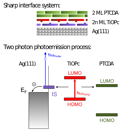
Figure 1: Schematic description of the model system studied and description of the two-photon photoemission process to investigate the electron dynamics at the molecular interface.
[1] L. Fernandez et al., Phys. Chem. Chem. Phys. 19, 2495 (2017)
Poster
Click reaction on the chiral PdGa{111} surfaces
1EMPA, Swiss Federal Laboratories for Materials Science and Technology, 8600 Dübendorf, Switzerland
2Institute of Condensed Matter Physics, Station 3, EPFL, 1015 Lausanne, Switzerland
Owing to the non-centrosymmetric nature of the P213 space group PdGa exists in two enantiomeric crystal forms A and B and all surfaces of this intermetallic compound (IMC) are chiral. This fact, together with the possibility to prepare atomically flat, well-ordered surfaces in ultra-high vacuum (UHV) enables the investigation of asymmetric chemical surface reactions in this system.
The stacking sequence of PdGa in the [111]-direction exhibits four non-equivalent atomic planes, therefore the (111) and (-1-1-1) surface terminations of the same crystal form are found to be structurally different. Specifically, one is terminated by a single, isolated Pd atom, accordingly denoted as Pd1, while the other reveals isolated Pd trimers as the top-most layer, referred to as Pd3 [1]. The chiral selectivity of Pd1 and Pd3 can be probed by adsorption of the prochiral 9-Ethynylphenanthrene (9-EP) molecule. On Pd1 a huge enantiomeric excess of 94-98% is found at room temperature (fig. 1b) [2], while for the same conditions a racemic mixture is observed on Pd3. Post-annealing to 490 K results in the dimerization of the 9-EP on Pd1, whereas on Pd3 9-EP propellers with a homochirality of 99% are formed (fig. 1c).
These results pave the way towards highly enantioselective, covalent coupling reactions. In view of the d-band model proposed by Nørskov et al [3], which links the catalytic activity to the position of the d-band center of the surface projected density of states (pDOS), a copper catalyzed Azide-Alkine Huisgen Cycloaddition was chosen as model reaction. Due to the copper-like d-band structure of Pd1 and Pd3 [1] this particular reaction of the click chemistry is expected to perform on PdGa{111} under UHV conditions as it was demonstrated with similar molecules on Cu(111) [4].
UHV conditions as it was demonstrated with similar molecules on Cu(111) [4]. Indeed, co-adsorption of 9-EP and 3-(4-Azidophenyl)propionic acid (APA) followed by post- annealing to 440 K lead to covalently coupled reaction products, whereas no reaction is observed on Pd3. The catalyzed reaction is regiostereoselective on Pd1 as it is on Cu(111), but on Pd1 one out of four enantiomeric forms of the reaction products is favored over the others.
On the other hand, on Pd3, the d-band model fails due to the big impact of the ensemble effect [5] on the reactivity for this particular reaction.
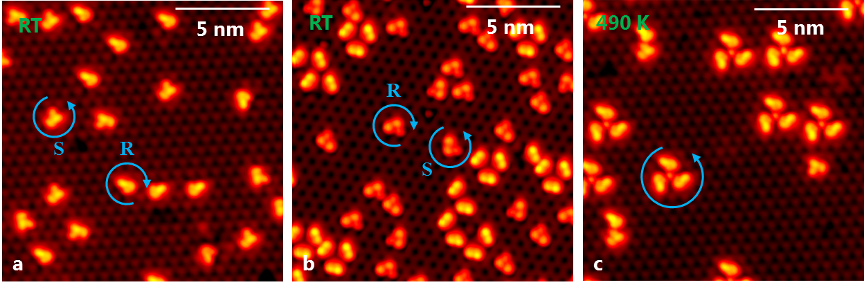
Figure 1: a) racemic mixture of 9-EP. b) enantioselective adsorption on Pd1. c) homochiral 9-EP propeller formation on Pd3.
[1] J. Prinz et al., Angew. Chem. Int. Ed. 51, 9339 (2012)
[2] J. Prinz et al., Angew. Chem. 127, 3974 (2015)
[3] J. K. Nørskov et al., Nature Chemistry 1, 37 (2009)
[4] F. Bebensee et al., J. Am. Chem. Soc. 135, 2136 (2013)
[5] W. M. H. Sachtler, Catal. Rev.: Sci. Eng. 14, 193 (1976)
Poster
Surface Structures of Niobium Oxide 2D Nanostructures and Ultrathin Films
1 Department of Materials, University of Oxford, Parks Road, Oxford, OX1 3PH, United Kingdom
Niobium oxides have been proposed in a wide variety of applications as catalysts, materials in microelectronics and as gas sensors. When metal oxides are grown as ultrathin films, consisting of only a few atomic layers in thickness, the interaction between the film and the substrate exerts a strong influence on the film structure. This can result in novel properties, such as enhanced catalytic reactivity. Modelling the structure of niobium oxide based catalysts also provides insight into catalytic mechanisms on the atomic level.
Niobium oxide nanostructures and ultrathin films were grown on reconstructed Au(111) surfaces. Following Nb deposition onto room temperature Au substrates, the samples were oxidised at 600 °C in 10-6 Pa oxygen to create epitaxial NbOx The phases obtained for the NbOx film included the honeycomb structure, triangular islands (Figure 1a), nanoclusters (Figure 1b) and a Moiré pattern, as observed by scanning tunneling microscopy (STM). Atomic movements have been observed in the triangular islands and nanoclusters. By using an image processing software package, Smart Align [1], distortions and errors in the STM images were corrected. The STM images are strongly enhanced by the software as the information of many frames can be condensed into one image.
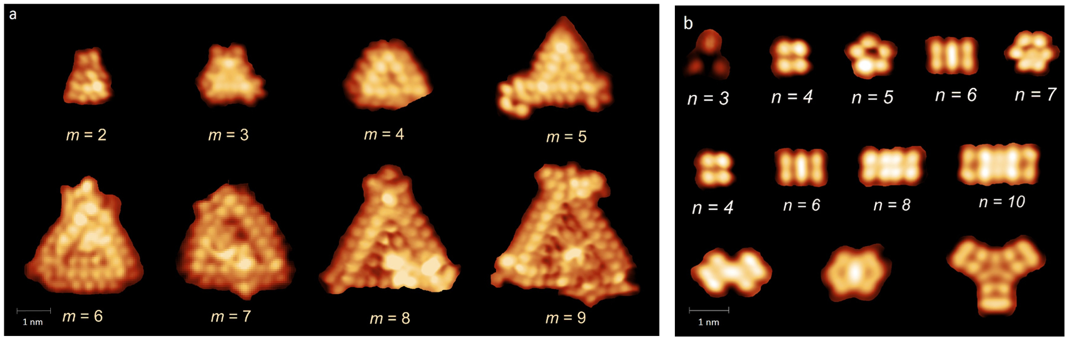
Figure 1: a) STM images of NbOx triangular islands of different sizes in the range m= 3-9 (Vs = 0.06-1.00 V, It = 0.24-0.26 nA). m denotes the atomic number in the inner sides of the islands. b) STM images of NbOx atomic clusters of different sizes. n denotes the atomic numbers in each cluster (Vs = 0.29-1.00 V, It = 0.18-0.24 nA).
[1] L. Jones et al., Advanced Structural and Chemical Imaging 1, 8(2015).
Poster
C60 adsorption on a two-dimensional oxide quasicrystal
1Martin-Luther-Universität Halle-Wittenberg, Halle, Germany
2Max-Planck-Institut für Mikrostrukturphysik, Halle, Germany
The recent observation of a two-dimensional oxide quasicrystal (OQC) at the interface to Pt(111) demonstrates that quasicrystalline structures can emerge in the heteroepitaxial growth of conventional periodic materials [1]. Under reducing conditions, a long-range ordered dodecagonal wetting layer is derived from ultrathin films of BaTiO3 at the threefold Pt(111) substrate. Atomically-resolved scanning tunneling microscopy (STM) images reveal the formation of a Niizeki-Gähler tiling as shown in Fig. 1a [2,3]. The contrast in the STM image is given by the sublattice of the Ti atoms. The atoms exhibit an arrangement of squares, triangles, and 30°C rhombs with a common edge length of 6.85 Å.
Due to the complexity of quasicrystalline materials, studies on the relation between aperiodic order and physical properties are challenging. Therefore, quasicrystal surfaces have been tested as templates for the growth of two-dimensional single element quasicrystals formed by molecular adsorbates. Recently, C60 and Pentacene were reported to exhibit quasicrystalline networks on icosahedral Al-Cu-Fe and Ag-In-Yb [4]. Here we report the first adsorption studies on the BaTiO3-derived OQC using C60 molecules. Their van-der-Waals diameter of 10 Å matches roughly the distance between two neighboring squares (9.35 Å, shown in Fig. 1b). Different coverages of C60 have been deposited on the OQC at room temperature and characterized by low-electron energy diffraction (LEED), x-ray photoemission spectroscopy (XPS), and STM. C60 molecules form hexagonal islands at the OQC surface or absorb at step edges, which indicates a weak interaction with the OQC substrate. With increasing coverages, second layer islands are formed well before the monolayer is completed. At temperatures of 510 K C60 thermal desorption sets in.
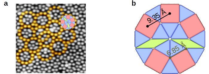
Figure 1: (a) STM image of BaTiO3-derived OQC at 77 K, 14x14 nm2, 30 pA, -0.15 V; (b) dodecagonal structure consist of squares, triangles, and rhombs with an edge length of 6.85 Å.
[1] S. Förster et al., Nature 502, 215 (2013).
[2] N. Niizeki and H. Mitani, J. Phys. A: Math. Gen. 20, L405 (1987).
[3] F. Gähler, in Quasicrystalline Materials (World Scientific, 1988).
[4] J. A. Smerdon et al., Nano Lett. 14, 1184 (2014).