
Click on the author name to see the abstract.
| 09:00-10:00 | Registration |
| 10:00-10:10 | Opening remarks |
| 10:10-10:50 | Repp |
| 10:50-11:15 | Sykes |
| 11:15-11:45 | Coffee break |
| 11:45-12:10 | Shimizu |
| 12:10-12:30 | Gaberle |
| 12:30-12:50 | Piquero |
| 12:50-13:10 | Jelinek |
| 13:10-16:30 | Lunch break and Poster Session |
| 16:30-16:55 | Lauritsen |
| 16:55-17:15 | Chen |
| 17:15-17:35 | Zandvliet |
| 17:35-17:55 | Bignardi |
Keynote
Individual Molecules on Surfaces: From Chemical Reactions to Ultra-Short Timescales
Department of Physics, University of Regensburg, 93040 Regensburg, Germany
We investigated different kind of π-conjugated molecules in a combined scanning tunneling (STM) and atomic force microscope (AFM). Whereas both measurement channels show features with sub-molecular resolution, the information they can provide is truly complementary. For example, STM allows the direct imaging of the unperturbed molecular orbitals [1], whereas the AFM channel directly reveals the molecular geometry [2, 3]. Further, we used the AFM-derived technique Kelvin probe force spectroscopy (KPFS) with sub-molecular resolution to image the polarity of individual bonds inside a single molecule [4].
The possibility of tailoring optical waveforms has allowed scientists to steer ultrafast electronic motion directly via the oscillating carrier wave of light - a principle dubbed "lightwave electronics" [5]. Despite tremendous interdisciplinary efforts to combine ultrafast temporal resolution with atomic spatial resolution, the ultrafast dynamics of individual molecular orbitals has remained out of reach.
Terahertz (THz) scanning tunnelling microscopy [6] (THz-STM) has introduced a new paradigm by combining STM with lightwave electronics. In THz-STM, the electric field of a phase-stable single-cycle THz waveform acts as a transient bias voltage across an STM junction. In analogy to the all-electronic pump-probe scheme introduced recently in STM [7] these voltage transients may result in a net current that can be detected by time-integrating electronics.
By means of a low-noise low-temperature lightwave-STM we entered an unprecedented tunnelling regime, where the peak of a terahertz electric-field waveform opens an otherwise forbidden tunnelling channel through a single molecular orbital. In this way, the terahertz peak removes a single electron from an individual pentacene molecule's highest occupied molecular orbital within a time window of ∼ 100 fs - faster than an oscillation cycle of the terahertz wave. This quantum process allowed us to capture a microscopic real-space snapshot of the molecular orbital on a sub-cycle time scale. By correlating two successive state-selective tunnelling events, we directly tracked coherent THz vibrations of a single molecule in the time domain [8].
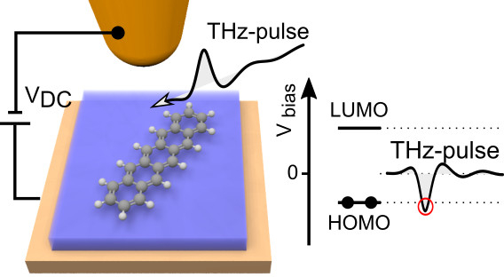
Figure 1: Schematic representation of the lightwave-STM setup, in which the THz-pulse acts as a bias transient.
[1] J. Repp et al., Phys. Rev. Lett. 94, 026803 (2005).
[2] L. Gross et al., Science 325, 1110 (2009).
[3] F. Albrecht et al., JACS 137, 7424 (2015).
Invited
Correlated Rotational Switching in 2D Self-assembled Molecular Rotor Arrays
1Department of Chemistry, Tufts University, Medford, MA 02155, USA
Molecular devices are capable of performing a number of functions from mechanical motion to simple computation. Their utility is somewhat limited, however, by difficulties associated with coupling them with either each other or with interfaces such as electrodes. Self-assembly of coupled molecular devices provides an option for the construction of larger entities that can more easily integrate with existing technologies. We demonstrate that ordered organometallic arrays can be formed spontaneously by reaction of precursor molecular rotor molecules with a metal surface. Scanning tunneling microscopy enables individual rotors in the arrays to be switched and the resultant switches in neighboring rotors imaged. The structure and dimensions of the ordered molecular rotor arrays dictate the correlated switching properties of the internal sub-molecular rotor units. Our results indicate self-assembly of 2D rotor crystals produce systems with correlated dynamics that would not have been predicted a priori.
These are highly emergent properties because individual, isolated molecular rotor units show random rotational behavior, whereas when coupled together in a self-assembled 2D crystal, correlated rotational switching is observed that would not have been predicted from the behavior of the individual units. The systems reported here are operated at low temperature, however, the barriers could be tuned via the design of the molecules themselves. While a lot is known about structure-function relationships in 3D crystals, 2D crystal engineering is still in its infancy. Moving forward, by measuring the properties of 2D crystals and then making subtle changes with organic synthesis, structure-function relationships can be drawn and emergent properties, like in this case correlated rotor switching, understood. This approach provides a new direction for the field of molecular machines, which while having produced a variety of single molecule devices, lacks ways to couple molecular motion between units and perform higher tasks.
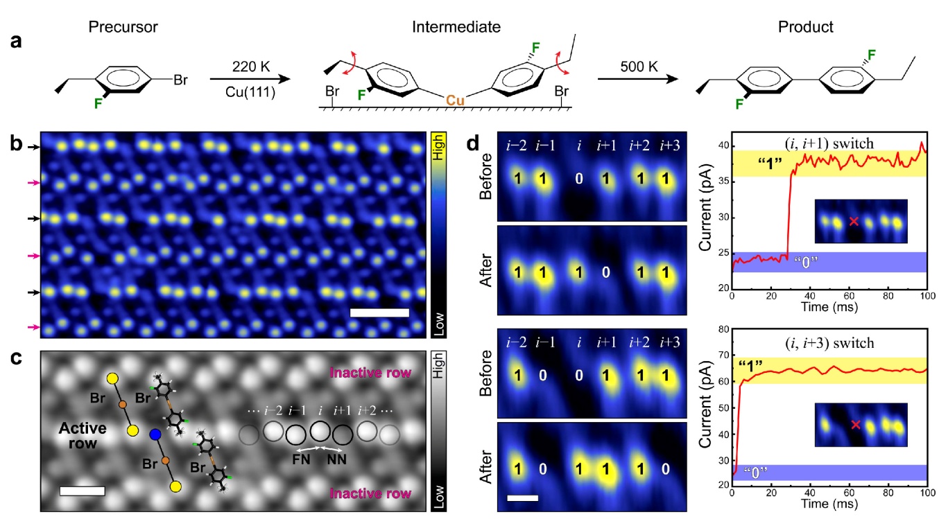
Figure 1: Correlated switching in self-assembled molecular rotor crystals.
Invited
Molecular adsorption on anatase TiO2(101) studied by submolecular imaging technique with Si cantilever AFM
1National Institute for Materials Science, Tsukuba, Japan
2JST-PRESTO, Saitama, Japan
3Dpto. de Física Teórica de la Materia Condensada, Universidad Autónoma de Madrid, Spain
Submolecular imaging using frequency-modulation (FM) atomic force microscopy (AFM) has recently been established as a stunning technique to reveal the chemical structure of unknown molecules, to characterize intra-molecular charge distributions, and to observe chemical transformations. So far, most of these feats were achieved on planar molecules using the so-called qPlus sensor, a specially designed quartz AFM sensor.
Here, we report a novel imaging method using multi-pass routine to achieve submolecular resolution on three-dimensional molecules and structures with a silicon (Si) cantilever-based AFM operated with large oscillation amplitudes. At variance with previous implementations, this method allows us to simultaneously image both intra-molecular structures and the atomic arrangement of the substrate [1]. Force volume measurements over C60 molecules clarify the validity of our method to achieve submolecular resolution. Using this technique as well as information obtained in our previous study of clean anatase TiO2(101) surface [2], we have investigated adsorption of pentancene molecules on terraces and steps of anatase TiO2(101) [3]. Based on comparison with theoretical calculations, we obtain an insight into substrate-molecule interaction and probe tip termination.
Figure 1: (a) Topographic AFM image and (b) multi-pass frequency shift image of pentacene molecules adsorbed on terraces and steps of the anatase TiO2(101) surface obtained at 77 K. Image size is 20nm×20nm.
[1] C. Moreno et al., Nano Lett. 15, 2257 (2015).
[2] O. Stesovych et al., Nat. Commun. 6, 7265 (2015).
[3] M. Todorovic et al., in preparation.
Contributed talk
Entropy Induced Changes in Molecular Adsorption Behaviour of Organic Molecules at Insulating Surfaces
1Physics and Astronomy, University College London, London, United Kingdom
2School of Maths and Physics, University of Lincoln, Lincoln, United Kingdom
3Advanced Institute for Materials Research, Tohoku University, Sendai, Japan
The adsorption of functionalised organic molecules on insulating surfaces plays an important role for many applications. However, studies so far have mainly focussed on the enthalpy of adsorption and uncertainties still remain about entropic contributions. Recent theoretical studies on the adsorption of individual flexible and rigid molecules on the KCl (001) surface have shown significant entropy loss during adsorption[1]. In this work we present data on molecular adsorption and diffusion of large organic molecules on terraces and step edges on the insulating KCl (001) surface, specifically focussing on the effects that molecular flexibility has on their dynamic behaviour and what implications that may have on self assembly.
Two functionalised organic molecules, 1,3,5-tri- (4-cyano-4,4biphenyl)-benzene (TCB) and 1,4-bis(cyanophenyl)-2,5-bis(decyloxy)benzene (CDB), were studied on the KCl (001) surface using density functional theory (DFT) and classical molecular dynamics (MD) simulations. MP2 calculations were used to benchmark the performance of Van der Waals corrected DFT-D3 calculations of adsorption energies and geometries and a classical force field was parameterised for each of the molecules using a genetic algorithm.[2] These force fields allowed us to perform long time-scale simulations to study the motion of molecules on the free energy surface.
In order to better understand adsorption of TCB and CDB molecules at non-zero temperatures, potential of mean force calculations were employed. It was found that entropic contributions significantly lower the adsorption free energy, which facilitated desorption. Furthermore, adhesion to step edges was investigated along with the associated change in entropy. While the flexible CDB molecule can readily adapt to step edges, the rigid TCB molecule is unable to and exhibits a significant entropy loss upon step adhesion. We show that the simple rigid rotor model can accurately estimate entropy loss upon step adhesion for TCB but fails for CDB. These results highlight how molecular flexibility directly influences surface dynamics, which can lead to different self-assembly growth modes.
[1] Gaberle J., Gao D. Z., Watkins M. B., and Shluger A. L., Calculating the entropy loss on adsorption of organic molecules at insulating surfaces, J. Phys. Chem. C 120, 3913-3921 (2016).
[2] Gao, D. Z., Federici Canova, F., Watkins, M. B., and Shluger, A. L.,Efficient parametrization of complex molecule-surface force fields, J. Comp. Chem. 36, 1187-1195 (2015).
Contributed talk
Precise engineering of quantum dot array coupling through their barrier widths
1Centro de Física de Materiales CSIC/UPV-EHU-MPC Manuel Lardizabal 5, E-20018 San Sebastián, Spain
2Instituto de Ciencia de Materiales de Aragón (ICMA), CSIC-Universidad de Zaragoza, E-50009 Zaragoza, Spain
3Department of Physics, Shahid Beheshti University, GC, Evin, 19839 Tehran, Iran
4Physics Department, Faculty of Science, Al-Azhar University, Nasr City, E-11884, Cairo, Egypt
5Department of Advanced Materials Science, The University of Tokyo, Chiba 277-8561, Japan
6Department of Physics, University of Basel, Klingelbergstrasse 82, CH-4056 Basel, Switzerland
Quantum dot (QD) arrays on surfaces, generated through molecular self-assembly processes, have so far provided researchers with a vast playground to study the electronic properties of new and exotic 2D materials in ultra-high-vacuum (UHV) conditions. By selecting the proper molecular constituents (tectons) and substrate, long-range ordered, periodic and robust nanoporous networks have been achieved, ranging from hydrogen-bonded to metal-organic structures [1]. Not only do they stand out as ideal templates for nanopatterning, but also as adequate candidates for studying fundamental physical phenomena such as confinement through the scattering of two-dimensional electron gases (2DEGs). Indeed, confinement tunability has already been accomplished by varying the pore (i.e. quantum dot) dimensions, geometrical shape and molecule substrate interactions [2,3]. In addition, inter-dot coupling has been shown by photoemission through the generation of new dispersive bands [4] that can be modulated through thermodynamics [5] and the condensation of guest elements (Xe atoms) [6].
To date, the modification of 2DEGs through inter-dot barrier width variations has not been experimentally demonstrated. Herein, sustained upon a combination of local scanning probes (STM/STS/AFM), angle resolved photoemission spectroscopy (ARPES) and extended model calculations, we show that we can precisely engineer the inter-dot barrier width by substitution of a single atom in a haloaromatic compound. As a result, we tune the confinement properties at each nanopore affecting the degree of QD intercoupling both on bulk and thin Ag films alike. These findings pave the way to reach full control over 2DEGs with the prospect of becoming key for future electronic devices.
Figure 1: Inter-dot barrier width engineering: single vs double molecular walls that tune the QD intercoupling properties.
[1] G. Pawin et al., Science 313, 961-962 (2006)
[2] S. Wang et al., Phys. Rev. B 88, 245430 (2013)
[3] F. Klappenberger et al., Nano Letters 9, 3509-3514 (2009)
[4] J. Lobo-Checa et al., Science 325, 300-303 (2009)
[5] I. Piquero-Zulaica et al., Applied Surface Science 391, 39-43 (2017)
[6] S. Nowakowska et al., Small 12, 3757-3763 (2016)
Contributed talk
Multiple electron charge states within a single molecule
1Institute of Physics, Czech Academy of Sciences Prague, Czech Republic
2Institute of chemistry and biochemistry, Czech Academy of Sciences Prague, Czech Republic
The field of molecular electronics aims at using a single molecule as building block for electronic devices. Ferrocene-based molecules are extremely appealing as they offer prospects of having a built-in charging functionality. They are known of being stable under redox states and therefore promising as candidates for quantum cellular automata units. Previous works demonstrated charging single metal adatoms [1], molecules or their clusters on insulating films [2] as well as charging of large self-assembled islands of molecules by STM or nc-AFM. [3]
Here we will present experimental evidence of controlling multiple charge states on a single 3,6,3',6'-tetraferrocene-9,9'bis-fluorenylidene, deposited on thin insulating NaCl film, by means of nc-AFM. We succeed to control the multiple charge states including their reversible transfer within a single molecule between different redox states. The induced charged states have prominent fingerprints in both the frequency shift and dissipation channels. Moreover, we demonstrate that the charge states can be modified by presence of neighboring charged molecules. The experimental evidence is corroborated with a theoretical model simulating response of a dynamically oscillating AFM probe to temporal changes of force due to the charging effects of molecules on surface.
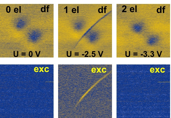
Figure 1: Frequency shift and dissipation signal images acquired for neutral, one and two-electron charge states of bis-ferrocene deposited on NaCl substrate.
[1] J. Repp et al., Science 305, 493 (2004)
Invited
Structure and electronic properties of single-layer MoS2 on Au(111)
1Interdisciplinary Nanoscience Center (iNANO), Aarhus University, Denmark
Single-layer MoS2 is one of the most studied of the two-dimensional transition metal dichalcogenides (TMDCs) as it was the first example of how a modified electronic structure reflected by a direct band gap and correspondingly different optical properties may develop when the TMDC becomes a single layer. Single-layer MoS2 can furthermore give rise to interesting new physics through the possibility of exploiting spin and valley degrees of freedom. We have developed a synthesis method that allows us to selectively form single-layer epitaxial MoS2 sheets grown with the (0001) basal plane in parallel to Au(111). This has the advantage of a well-defined and well-oriented system that enables us to systematically address the structural and electronic features pertaining to such single MoS2 layers on a metal support using scanning tunneling microscope (STM) and angle-resolved photoemission spectroscopy (ARPES). Coherent sheets of MoS2 at varying surface coverage can be formed by sequences of reactive physical vapor deposition of Mo in a H2S atmosphere followed by post annealing in the sulfiding atmosphere. Structurally, the single-layer MoS2 adopts a large characteristic superstructure due to the lattice mismatch, reflected by a moiré pattern in STM images [1,2]. Our DFT studies furthermore reveal that this modulation is influenced by the preferential bonding of the bottom S in the MoS2 sheet to on-top positions on the Au(111). The ARPES results [3] show that the Au-supported single-layer MoS2 retains the important direct band gap at the K point seen in free-standing single-MoS2, whereas the out-of-plane S bonding to Au leads to some distortions of the band near the Γ point. By varying the synthesis conditions we can furthermore study isolated MoS2 islands as well as stacking faults at the interface between MoS2 patches. This approach in particular allows us to address the edges terminating the MoS2 sheets, which are found in photoemission and STM studies to be metallic due to the presence of edge states in contrast to the semiconducting basal plane
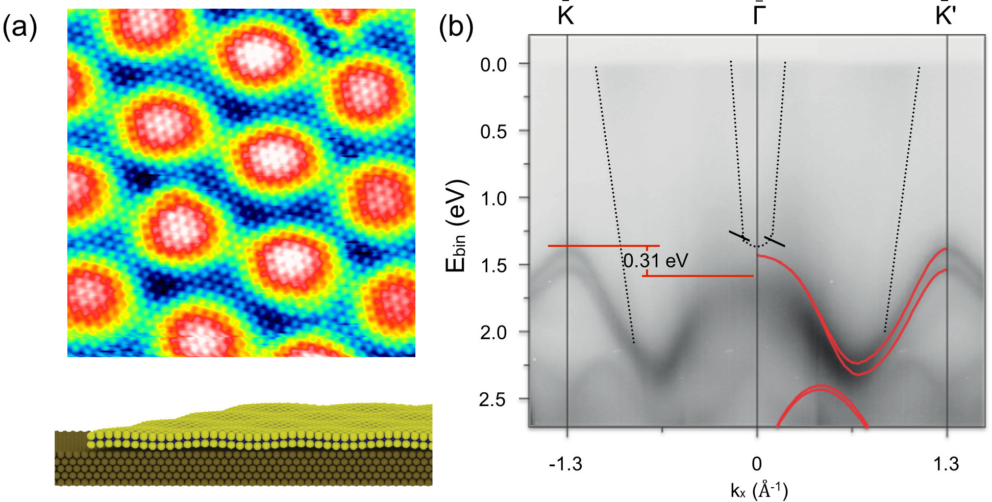
Figure 1: (a) Atom-resolved STM image showing the atomic lattice and moiré pattern of MoS2/Au(111) (b) Photoemission results along the Γ-K direction for MoS2/Au(111).
[1] S.G. Sørensen, H.G. Füchtbauer, A.K. Tuxen et al., ACS Nano 8, 6788 (2014).
[2] S.S. Grønborg, S. Ulstrup, M. Bianchi et al., Langmuir 31, 9700 (2015).
[3] J.A. Miwa, S. Ulstrup, S.G. Sørensen et al., Phys. Rev. Lett. 114, 046802 (2015).
Contributed talk
Synthesis and Characterisation of Epitaxial MoS2 Nanocrystals
1 Department of Materials, University of Oxford, Parks Road, Oxford, United Kingdom
Two-dimensional (2D) nanocrystals of molybdenum disulphide (MoS2) are grown on the substrate strontium titanate (SrTiO3) by chemical vapour deposition (CVD). MoS2 is an indirect-bandgap material in its bulk form, and exhibits an indirect-to-direct transition when thinned to a monolayer. It also possesses metallic edge states due to the shape finiteness. As a 2D material, MoS2 is highly sensitive to its substrates, so engineering the substrate is an important step to be able to manipulate it and fully realise its potentials. However, it has only been studied on very few substrates, e.g. Au [1] and Si/SiO2 [2]. In this project, nanocrystals of MoS2 are grown on reconstructed SrTiO3 surfaces.
The new substrate is crystalline and each crystal surface (e.g. (111) and (110)) has a wide range of surface reconstructions [3,4], which were prepared by high-temperature annealing (800-1200°C) in either ultra-high vacuum (UHV) or partial pressures of oxygen. Their near-atomic structures were imaged by scanning tunnelling microscopy (STM). The different surfaces possess different lattice constants and surface energies, which could influence the epitaxy of the nanocrystal growth.
The structural, electronic and optical properties of MoS2 grown on SrTiO3 are being characterised by STM, ultra-high vacuum (UHV) scanning electron microscopy (SEM), photoluminescence (PL) and Raman spectroscopy. The good epitaxial relationship between MoS2 crystals and SrTiO3 has been noted by SEM and STM (Figure 1), the latter of which also recorded the atomic structure and Moiré patterns of MoS2. PL and Raman results confirmed the monolayer thickness of the crystals and their good optical properties. They also provided information on the strain and doping levels in the nanocrystals induced by the substrate. It is expected that the new substrate will result in interesting new properties of dichalcogenides and help us explore their new applications in 2D nanodevices.
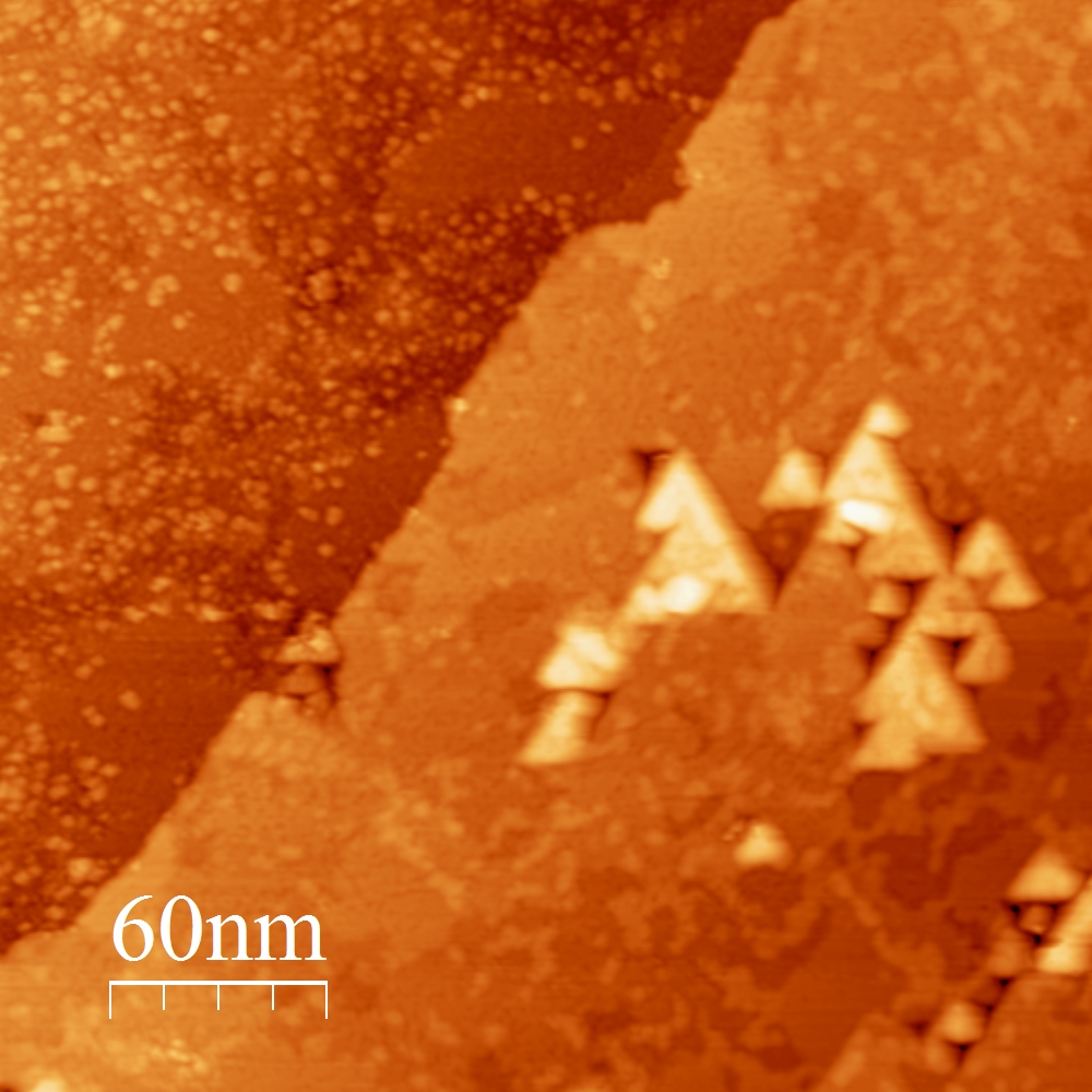
Figure 1: Figure 1: STM images of MoS2 nanocrystals (bright triangles) on SrTiO3(111).
[1] M. Buscema et al., Nano Res. 7, 561(2014).
[2] S. Bhattacharjee et al., IEEE Trans. Electron Devices 63, 2556(2016).
[3] B. Russell et al., J. Phys. Chem. C 112, 6538(2008).
[4] B. Russell et al., Phys. Rev. B 77, 245414(2008).
Contributed talk
Germanene: the germanium analogue of graphene
1Physics of Interfaces and Nanomaterials and MESA+ Institute for Nanotechnology, University of Twente, P.O. Box 217, 7500AE Enschede, The Netherlands
Recently, a few research groups have reported the growth of germanene, a new member of the graphene family [1]. Germanene is in many aspects very similar to graphene, but in contrast to the planar graphene lattice, the germanene honeycomb lattice is slightly buckled and composed of two vertically displaced sub-lattices. Frist principles total energy calculations have revealed that free-standing germanene is a two-dimensional Dirac fermion system, i.e. the electrons behave as massless relativistic particles that are described by the Dirac equation, i.e. the relativistic variant of the Schrödinger equation. We will give a brief update of the growth and electronic properties of germanene on Pt/Ge(110) nanocrystals [2,3]. Subsequently, we will show that large and continuous single germanene layers can be grown on molybdenum disulfide (MoS2) [4]. The structural and electronic properties of the germanene layer are studied with scanning tunneling microscopy and spectroscopy. The lattice constant of the germanene layer is 3.8 ± 0.1 Å , i.e. substantially larger than the lattice constant of MoS2 (3.16 Å), and the interlayer distance between the germanene layer and the MoS2 substrate is 3.2 ± 0.2 Å, suggesting that we are dealing with a low-buckled germanene layer. The density of states of the germanene layer exhibits a V-shape, which is reminiscent for a two-dimensional Dirac system. The minimum of the density of states is located near the Fermi level.
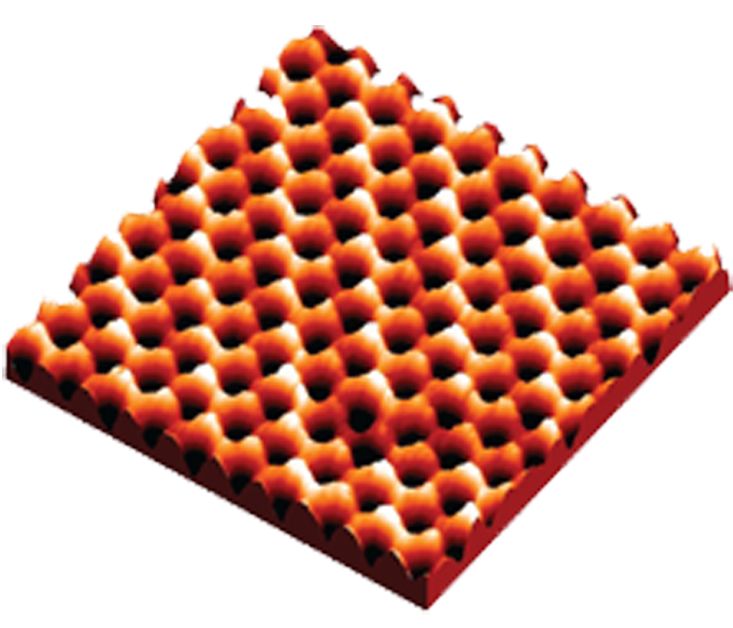
Figure 1: Scanning tunneling microscopy image (4.5 nm by 4.5 nm) of buckled honeycomb lattice of germanene. Sample bias -0.5 V, tunnel current 0.2 nA.
[1] A. Acun et al., J. Phys. Cond. Mat. 27, 443002 (2015) and references therein.
[2] P. Bampoulis et al., J. Phys. Cond. Mat. 26, 442001 (2014).
[3] L. Zhang et al., Appl. Phys. Lett. 107, 111605 (2015).
[4] L. Zhang et al., Phys. Rev. Lett. 116, 256804 (2016).
Contributed talk
Key Role of Rotated Domains in Oxygen Intercalation at Graphene on Ni(111)
1Elettra - Sincrotrone Trieste, s.s. 14, km 163.5, 34149 Basovizza, Trieste, Italy
2Università degli Studi di Trieste, via Valerio 2, 34127 Trieste, Italy
3Istituto Officina dei Materiali - CNR, s.s. 14, km 163.5, 34149 Basovizza, Trieste, Italy
4Istituto dei Sistemi Complessi - CNR, via dei Taurini 19, 00185 Roma, Italy
n this contribution I will provide a description of the oxygen intercalation at the strongly interacting graphene on Ni(111) and of the role of rotated graphene domains in triggering the intercalation. The system was studied by a combination of high-resolution x-ray photoelectron spectroscopy (HR-XPS), photoelectron diffraction (XPD) and angle-resolved photoemission (ARUPS) performed with synchrotron radiation. The HR-XPS measurements provided a full characterization of the interface at each stage of the intercalation, revealing the formation of an oxide layer between graphene and the metal substrate. The ARUPS data showed that the oxide layer efficiently decouples graphene from the substrate, restoring the Dirac cone and providing a slight n-doping. The C1s XPD measurements revealed that the graphene domains not aligned with the Ni substrate are the first to be intercalated with oxygen. At the same time, these domains are also preferential regions under which the oxygen is retained during the deintercalation process.