Click on the author name to see the abstract.
| 10:00-10:40 | Sánchez-Portal |
| 10:40-11:05 | Africh |
| 11:05-11:35 | Coffee break |
| 11:35-12:00 | Chuvilin |
| 12:00-12:20 | Gastaldo |
| 12:20-12:40 | Balog |
| 12:40-13:00 | Menzel |
| 13:00-15:00 | Lunch break |
| 15:00-15:20 | Zamborlini |
| 15:20-15:40 | Sarasola |
| 15:40-16:00 | Soubatch |
| 16:00-16:20 | Woodruff |
| 16:20-16:50 | Coffee break |
| 16:50-17:15 | Magnussen |
| 17:15-17:40 | Sulpizi |
| 17:40-17:50 | Concluding remarks |
Keynote
Towards electronic devices using graphene nanoribbons
1CFM CSIC-UPV/EHU and DIPC, Paseo Manuel de Lardizabal 5, E-20018, San Sebastián, Spain
2ICMAB-CSIC, Campus de la UAB, E-08193 Bellaterra, Spain
3IKERBASQUE, Basque Foundation for Science, E-48013, Bilbao, Spain
In this talk, I will present some studies of prototype electron devices made out of graphene nanoribbons that we have recently performed in our group in San Sebastián. In collaboration with our experimental colleagues, we have studied the properties of armchair GNRs (AGNRs) doped and functionalized in different ways. In particular, we have studied 7-AGNRs periodically doped with boron pairs on Au(111), and compared our findings with scanning tunneling microscopy/spectroscopy (STM/STS) and angle-resolved photoemission (ARPES) data. Furthermore, it is possible to grow structures formed by pristine segments separated by regions doped with B pairs [1]. We have studied the properties of such boron defects as scattering centers for GNR electrons, and found that they provide large effective barriers for the propagation of electrons in the valence band (VB), but are nearly transparent for the immediately lower energy band (VB-1) due to the different symmetry of both bands. As a result, the VB gives rise to quantized levels in the pristine regions that are clearly identified (see the Figure), with a remarkable agreement between theory and experiment [1].
From a purely theoretical perspective, we have explored a prototype 4-terminal semiconducting device formed by two crossed AGNRs as a function of the intersection angle, stacking, inter-GNR separation, GNR width, and voltage. [2] Interestingly, when the AGNRs intersect at θ=60° electrons injected from one terminal can be split into two outgoing waves with a tunable ratio around 50% and with almost negligible back-reflection. The split electron-wave is found to propagate partly straight across the intersection region in one ribbon and partly in one direction of the other ribbon, i.e., in analogy of an optical beam splitter. We rationalize our findings with a simple model that suggests that electronic beam splitters can generally be realized with crossed GNRs.
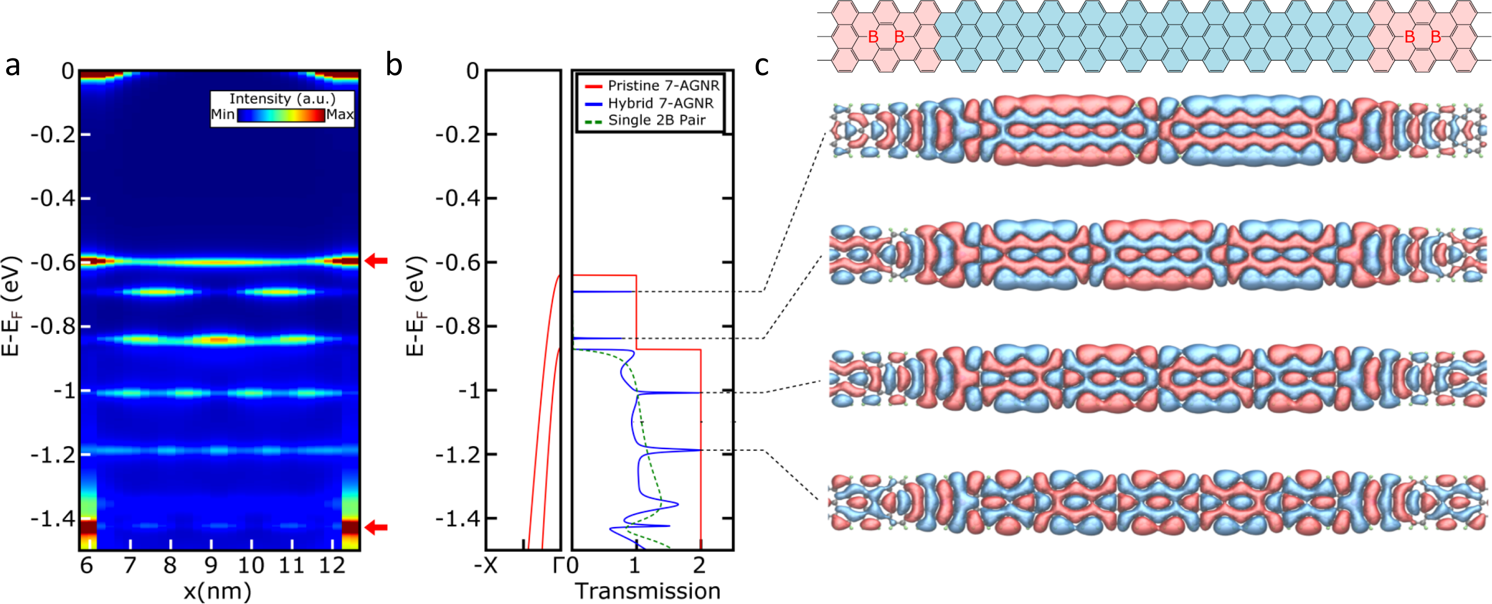
Figure 1: (a) Calculated projected density of states in a pristine segment between two borylated units 65Å apart. (b) Dispersion of the VB and VB-1 bands and the corresponding transmission curves for a pristine 7-AGNR (red line), a 7-AGNR containing an isolated B-pair defect (green doted line), and a 7-AGNR containing two B-pairs separated by 65Å (blue line exhibiting characteristic Fabry-Perot-like resonances). (c) Scheme and real part of the transmission eigenchannels with an increasing number of nodes as we move down in energy.
The authors acknowledge financial support from FP7 FET-ICT project No. 610446 project, EU H2020 project No. 676598, MINECO (Grant No. MAT2013-46593-C6-2-P), the Basque Dep. de Educación and the UPV/EHU (Grant No. IT-756-13).
[1] E. Carbonell-Sanroma, et al., Nano Letters 17, 50-56 (2017)
[2] P. Brandimarte, et al., J. Chem. Phys. 146, 092318 (2017)
Invited
In-situ atomic-scale investigation of CVD-grown graphene on polycrystalline nickel substrates
1IOM-CNR Laboratorio TASC, Area Science Park, s.s. 14 km 163.5, Basovizza, 34149 Trieste, Italy
2The Abdus Salam International Centre for Theoretical Physics, Strada Costiera 11, 34151 Trieste, Italy
3Department of Physics, University of Trieste, Via Valerio 2, 34127 Trieste, Italy
The understanding of growth mechanisms, at the atomic level and on substrates suitable for scalable CVD production, is a key step for the use of graphene in industrial applications. However, most studies so far are based on the interpretation of post-growth experiments on model surfaces, which can sometimes be misleading.
By means of variable-temperature scanning tunnelling microscopy, we studied the graphene growth process in the 380-500°C temperature range with a time resolution down to 100 ms/image and on commercially available polycrystalline Ni substrates. (111) and (100) facets were identified in the examined regions of the polycrystalline sample and growth mechanisms were investigated on both flat (100) terraces and highly-stepped regions. On flat terraces, graphene can grow directly on top of the metal or via in-plane carbide conversion, as already evidenced in our previous work on model (111) substrates [1]. On (100) grains, a variety of moiré superstructures are present, which can be well explained in atomistic models by the mismatch with the substrate and whose appearance in the STM images is well reproduced by density functional theory simulations. These moiré structures were found to be able to influence carbide segregation under graphene, thus providing a new route to tune its electronic properties on a nano-meter scale. Furthermore, with the aid of an add-on FAST module allowing for the acquisition of STM time-series up to video rate, novel growth mechanisms at stepped areas are unveiled, which rationalize the continuity of the graphene layer even when it lies on highly stepped polycrystalline substrates.
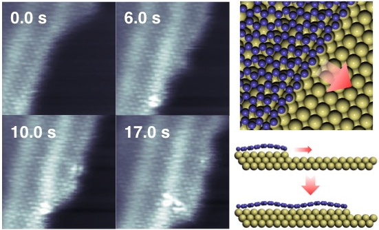
Figure 1: Graphene growth on (100) Ni facets. Left: selected frames of an atomically resolved Fast-STM movie during growth at 450°C; Right: atomistic model of the mechanism imaged on the left
[1] L.L. Patera et al., ACS Nano 7, 7901-7912 (2013).
Invited
Accessing kinetics of structural rearrangements in graphene via direct atomic imaging
1CIC nanoGUNE Consolider, Tolosa Hiribidea 76, 20018 Donostia-San Sebastián, Spain
2IKERBASQUE Basque Foundation for Science, María Díaz de Haro 3, E-48013 Bilbao, Spain
The raise of nanoscience and nanotechnology and necessity to characterize the structure of individual objects consisting of a countable number of atoms determined the shift of structure characterization paradigm from bulk methods like X-ray diffractometry to local high resolution methods like electron microscopy. The similar shift in paradigm is urging now in chemistry - chemical processes defining structure and properties of nanoscale and low dimensional objects often constitute a negligible part of the total volume of the material, and thus their assessment by experimental bulk chemical methods if often impossible. The new concept is provided by the time resolved electron microscopy allowing for direct observation of atomic rearrangements.
We are developing the methodology to apply the formalism and approaches of the classical chemical kinetics for the quantitative description of atomistic processes observable in the microscope. We show that a proper statistical treatment of the data obtained in a range of experimental conditions allows determining the threshold energies for radiation induced reactions. But not only that: we show that true activation energies for thermally activated reaction pathways for individual defects can be estimated as well.
We apply this methodology for reactions of point defects in graphene. The cross-sections and threshold energies of irreversible (atom emission) and reversible (bond rotation, see Figure 1) processes are measured. Observation of statistically significant number of events at variable experimental conditions allows decoupling of radiation induced and thermal reaction pathways and obtaining independent estimations of cross-sections and activation energies for direct and backwards rotations. The cross-sections of direct rotation were found to be in a decent agreement with theoretical estimations. Interestingly the backwards rotation is characterized by very high cross-section exceeding theoretical values by 3-4 orders of magnitude. The values obtained rule out electron nucleus collisions as the main pathway of energy transfer from electron beam to the sample. We speculate that the energy is transferred through electron-electron interactions via strong coupling of excited electron states with the phonon modes localized around the defect.
Acknowledgements: The contribution of my co-workers from Nottingham University, KAUST, Novosibirsk Institute of Inorganic Chemistry, Vienna University and Graphenea Company is greatly appreciated. The work was partially supported by collaboration project with FEI Company and by FP7-PEOPLE-2011-IRSES N295180 (MagNonMag) project.
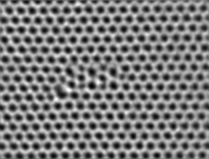
Figure 1: The reaction of C-C bond rotation (Stone-Wales transformation) determines transformations and mobility of the whole range of topological defects in graphene.
Contributed talk
Topological line defects in graphene nanoislands
1Department of Physics, Federal University of Minas Gerais, Belo Horizonte 31270-901, Brazil
2Catalan Institute of Nanoscience and Nanotechnology (ICN2), CSIC and The Barcelona Institute of Science and Technology, Campus UAB, Bellaterra, 08193 Barcelona, Spain
3Centro de Desenvolvimento da Tecnologia Nuclear (CDTN/CNENS) Belo Horizonte/ Brazil
4Donostia International Physics Center (DIPC), Paseo Manuel de Lardizabal 4, E-20018, Donostia, Spain
5IKERBASQUE, Basque Foundation for Science, E- 48011 Bilbao, Spain
6ICREA - Institució Catalana de Recerca i Estudis Avançats, Lluis Companys 23, 08010 Barcelona, Spain
Understanding grain boundaries in polycrystalline graphene is crucial for the control of both their electronic and mechanical properties. Depending on their topological structure, boundaries can impede transport across grains, or host their own one dimensional metallic states [1]. Concerning mechanical stability, they can either weaken or strengthen the graphene sheet [2]. We here report experimental evidence on some predicted and other new topological defect boundary structures, as found by Scanning Tunnelling Microscopy (STM) in graphene nanoislands grown on Ni(111) by CVD. By using mild annealing temperatures, we obtain multi-domain nanoislands with different types of domain boundaries. High-resolution STM images allow us to characterize both the stacking and orientation of graphene domains and the boundary atomic structure. From a statistical analysis of the rotated domains, we conclude that their abundance is closely related to the boundary energetics [3], evidencing that the selection of rotational domains is determined by boundary rather than stacking energetics. linear and ring boundaries separating 30º rotated domains are particularly interesting: the linear ones are predicted to be transparent to Dirac electrons [4], whereas confined resonances have already been observed in quantum dots bound by similar ring boundaries [5].
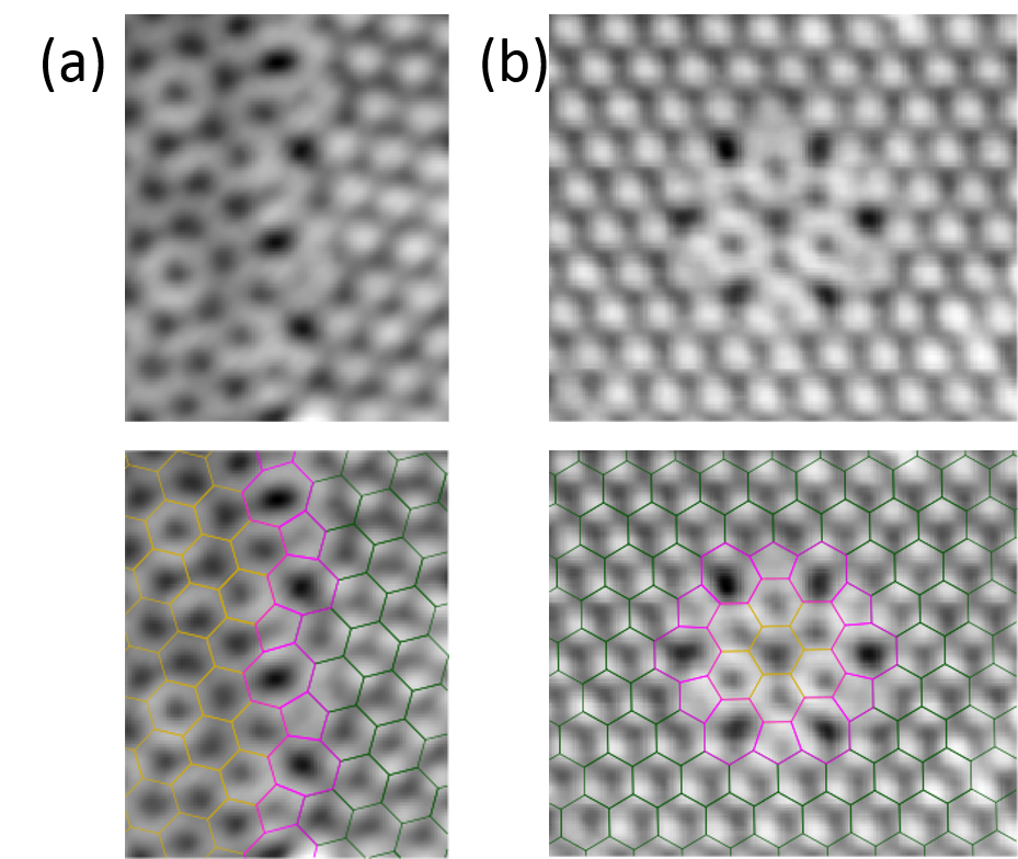
Figure 1: a) STM image of a zoomed area of a graphene nanoislands grown on Ni(111) by CVD. Different type of topological defect boundaries consisting on pentagon/heptagon units separate stripes (a) and quantum dots (b) of domains with 30° of relative rotation.
[1] A. Luican-Mayer et al., 2D Materials 3, 031005 (2012); J. Lahiri et al., Nature Nanotech. 5, 326 (2010)
[2] Y. Wei et al. Nature Mater. 11, 759 (2012)
[3] O. Yazyev et al., Phys. Rev. B 81, 195420 (2010)
[4] O. Yazyev et al., Nature Mater. 9, 806 (2010)
[5] E. Cockayne et al., Phys. Rev. B 83, 195425 (2011)
Contributed talk
Switching the reactivity of graphene on Ir(111) by hydrogen intercalation
1Dept. of Physics and Astronomy, University of Aarhus, Aarhus C, Denmark
2iNANO, University of Aarhus, DK-8000 Aarhus C, Denmark
The functionalization of graphene with hydrogen enables a variety of new phenomena to appear such as e.g. band-gap opening[1], enhanced spin-orbit coupling [2] and ferromagnetic order in single sided hydrogenated graphene [3]. The appearance of these phenomena, however, strongly depends on the type of hydrogen structures, formation of which is often driven by the graphene-substrate interactions. [4,5] Moreover, the possibility for graphene to act as a hydrogen storage medium has led to several studies[6,7].
Using XPS and STM techniques we show that quasi free-standing graphene can be prepared on Ir(111) upon hydrogen intercalation. The intercalation in turn modifies how graphene reacts towards atomic hydrogen bombardment - resulting in formation of different type of hydrogen structures when compared to the non-intercalated case. In addition, I will show that while graphene on Ir(111) can be functionalized upon exposure to vibrationally excited H2#, [8] its reactivity is fully suppressed in quasi free-standing state that is achieved by intercalation. Understanding the reactivity of graphene towards hydrogen and the role of underlying substrates in these reactions is important for the realization of carbon-based hydrogen storage materials.
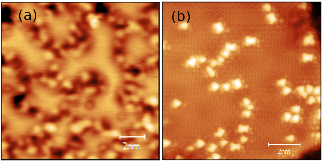
Figure 1: Comparison of hydrogen structures formed on a) bare graphene and b) hydrogen intercalated graphene on Ir(111).
[1] R. Balog, et al., Nature Materials. 9, 315 (2010)
[2] J. Balakrishnan, et al., Nat Phys. 9, 284 (2013)
[3] A. J. M. Giesbers, et al., Phys. Rev. Lett. 111, 166101 (2013)
[4] J. Jorgensen, et al., ACS Nano 10, 10798 (2016)
[5] R. Balog, et al., ACS Nano 7, 3823 (2013)
[6] H. McKay, et al., Phys. Rev. B 81, 075425 (2010)
[7] Y. Miura, et al., J Appl. Phys. 93, 3395 (2003)
[8] L. Kyhl, et al., (in preparation)
Contributed talk
Core hole clock characterization of intercalated and compressed argon under graphene monolayers and in blisters.
1 Elettra - Sincrotrone Trieste, AREA Science Park, S.S. 14 km 163.5, 34149 Trieste, Italy
2 CNR-ISC Istituto dei Sistemi Complessi, Via Fosso del Cavaliere 100, 00133 Roma, Italy
3 Physikdepartment E20, Technische Universität München, 85748 Garching, Germany
4 Fritz-Haber Institut der MPG, 14195 Berlin, Germany
Recently it has been shown by several groups[1-4] that argon can be stably intercalated and compressed into bubbles or blisters under graphene (Gr) monolayers on metal substrates. On the basis of our previous definition of these states by XPS, XAS, and STM [4], we now investigated the state of the argon atoms under Gr on Ni(111) by resonant core excitation and decay, the so-called core hole clock (CHC) method [5,6], using XPS as the transfer standard. For intercalated Ar monolayers the Ar 2p3/2→4s resonance is not detected at all; the weak decay signal consists of Auger electrons only. Both these findings indicate that the core exciton state is quenched or possesses extremely fast decay. For compressed Ar in blisters containing more than 1 Ar layer a small resonance is found which decays into Auger states; for blisters containing several Ar monolayers (at least mono, bi and trilayers) a stronger, shifted resonance is detected which leads to only spectator decay electrons. We discuss these results in terms of distinguishable contributions from Ar atoms pressed into the Ni substrate, Ar in contact with the graphene cover, and those Ar atoms shielded from both interfaces in the interior of blisters. These results corroborate the interpretations given before from XPS, XAS, and STM results and contribute to the understanding of both the Ar blisters and the physics of excitation decay in strongly coupled systems.
Time permitting some interesting further details and extensions to other systems will be reported.
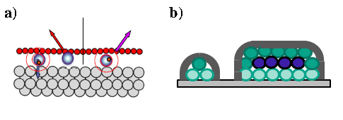
Figure 1: a) Scheme of the excitation-decay process for an intercalated Ar atom under a Gr ML, with decay after (left) and before (right) charge transfer. b) Schematics of the three different Ar states in a Gr blisters, and their contacts to metal and/or Gr enclosure, or shielded from both.
[1] C. Herbig et al., Phys. Rev. B 92, 085429(2015).
[2] F. Späth et al., Surf. Sci. 643, 222(2016); doi: 10.1016/j.susc.2015.05.009.
[3] G. Zamborlini et al., ACS Nano Lett. 15, 6162(2015); doi: 10.1021/acs.nanolett.5b02475.
[4] R. Larciprete et al., ACS Nano Lett. 16, 1808(2016); doi: 10.1021/acs.nanolett.5b04849.
[5] For a review, see P.A. Brühwiler, O. Karis, and N. Martensson, Rev. Mod. Phys. 74, 702(2002).
[6] For a recent survey, see D. Menzel, Chem. Soc. Rev. 37, 37(2008), and references therein.
Contributed talk
Unexpected multi-orbital charge transfer at highly oriented organic/metal interfaces
1Peter Grünberg Institute (PGI-6), Forschungszentrum Jülich GmbH, Jülich, Germany
2Elettra - Sincrotrone Trieste S.C.p.A., 34149 Trieste, Italy
3Institut für Physik, Karl-Franzens-Universität Graz, 8010 Graz, Austria
4CNR-IOM Laboratorio Nazionale TASC, Basovizza SS-14, km 163.5, I34012 Trieste, Italy
5Department of Physics, University of Trieste, via A. Valerio 2, 34127 Trieste, Italy
Supramolecular multiporphyrin arrays are considered ideal model systems for the study of energy transfer mechanisms and of natural photosynthesis [1]. A reliable and rigorous method is needed, in order to characterize the electronic and structural properties of porphyrins at the interface, where the molecule-substrate interactions play a fundamental role. We investigate the adsorption behavior of nickel tetraphenyl porphyrin (NiTPP) molecules on the Cu(100) surface by applying a comprehensive multi-technique approach, photoemission electron microscopy (PEEM), photoemission tomography (PT) and STM, complemented density functional theory (DFT) calculations.
The adsorbed NiTPP arrange in two different geometrical configurations with different orientation respect to [100] crystal direction. By combining STM with DFT calculations, we demonstrate that the contrast, in STM images, arises mainly from the phenyl peripheral groups, which are tilted upwards. This adsorption configuration prevents the macrocycle, where frontier orbitals are localized, to be resolved by the STM tip.
For this reason, STM cannot be used for mapping the charge distribution of the highest occupied and lowest unoccupied molecular orbitals (HOMO and LUMO, respectively). Therefore, as a complementary technique, we exploited the capability of our PEEM to directly image a wide reciprocal space in one single shoot. The angle-resolved photoemission data (ARPES) were then compared to DFT calculations, within the PT framework [2]. The molecular orbitals (MO) exhibit peculiar features which can be used to unambiguously identify them in the valence band spectra. This is particularly useful to determine the molecule-substrate interaction and the charge transfer phenomena between adsorbed molecules and metal surfaces. The comparison between experiment and theory shows that the former gas-phase LUMO+3 becomes occupied upon adsorption on the metal surface (see Fig1 c). This unexpected result suggests that a multi-technique approach is mandatory in order to obtain a consistent picture of the adsorption behavior and electronic properties of the molecular system.
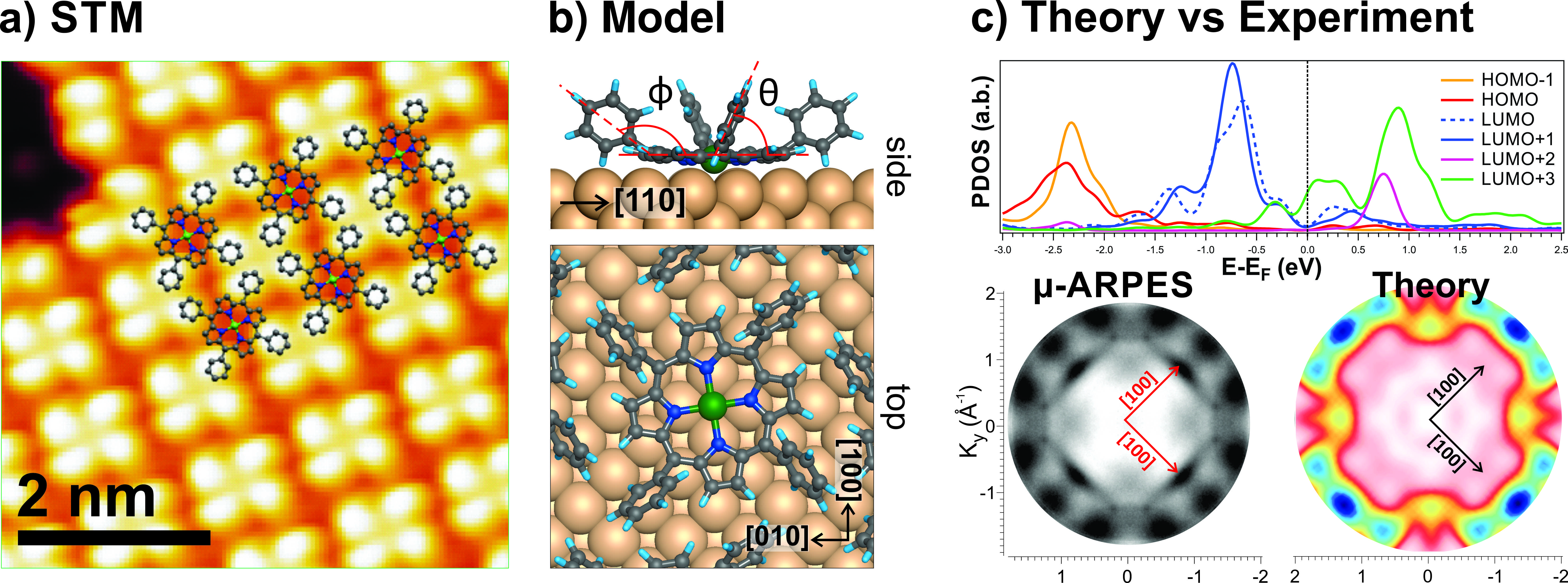
a) STM image of the NiTPP/Cu(100). b) Proposed absorption model for NiTPP/Cu(100). c) top: Projected density of state of MOs for NiTPP/Cu(100). Bottom: comparison between ARPES and DFT calculations.
[1] N. A. Rakow, K. S. Suslick, Nature 406, 710 (2000).
[2] P. Puschnig et al., Nature 326, 702 (2009).
Contributed talk
On the origin of unexpected core level shifts of tetrapyrrole molecules on surfaces
1University of the Basque Country UPV/EHU, Donostia, Spain
2Donostia International Physics Center (DIPC),Donostia, Spain
3Material Physics Center CFM, Donostia, Spain
4Columbia University, New York, USA
5CNR-IOM, Trieste, Italy
6IKERBASQUE, Bilbo, Spain
Several studies have addressed the presence of unexpected components in the molecular level X-ray Photoelectron Spectroscopy (XPS) spectra, specially in the N1s signal, when tetrapyrrole molecules are deposited on different surfaces in Ultra High Vacuum (UHV) conditions[1-3]. In this work, we employ a set of DFT-based tools to unravel the origin of an unpredicted peak in the N1s core level spectra of metal phthalocyanines (in particular, ZnPc) adsorbed on Cu(110). We analyze the different possible chemical or electronic mechanisms that might explain this experimental result. On one hand, we prove that surface effects, such as LUMO splitting and surface screening, cannot account for the huge experimental CLSs. On the other hand, we show that, when adsorbed at low temperatures, these molecules capture residual H atoms from the surface, giving rise to hydrogenated molecular species without de-metalation of the molecule and, thus, to an extra component in the molecular CLS spectra.[4] Only upon annealing, and subsequent H release, do the molecules recover their nominal structural and electronic properties. Our results thus demonstrate that residual hydrogen, which is known to be the primary residual gas in UHV systems, might have a significant effect on the measured electronic properties of molecule-surface complexes.
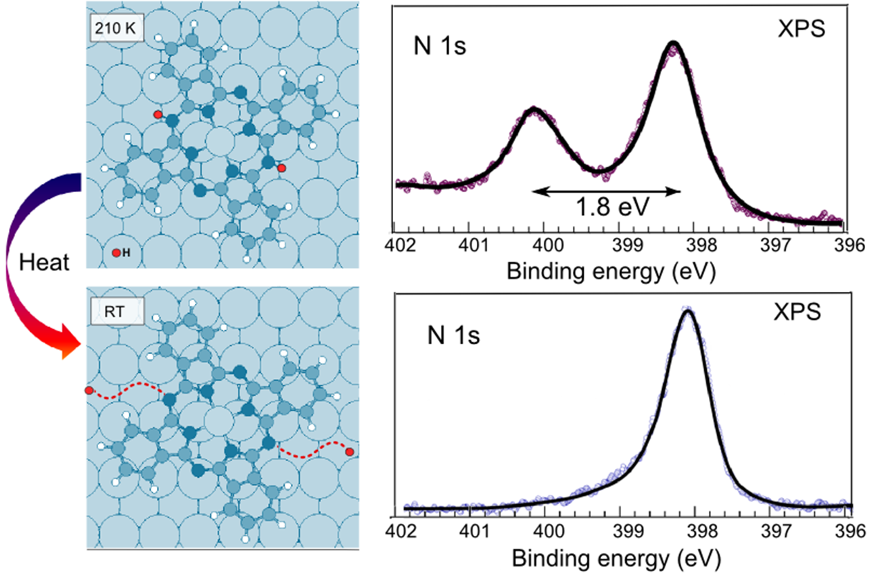
Figure 1: Left side: Dehydrogenation of adsorbed organic molecules upon annealing. Right side: Corresponding XPS spectra prior and after annealing.
[1] A. Garcia-Lekue et al., J. Phys. Chem C 116, 15378 (2012)
[2] S.Yu et al. J.Chem.Phys. 136, 154703 (2012)
[3] G. Lovat et al., Phys. Chem. Chem. Phys. 17, 30119 (2015)
[4] A.Sarasola et al., submitted
Contributed talk
1D and 2D extended materials on metal surfaces: Interface structure with NIXSW
1Peter Grünberg Institut (PGI-3), Forschungszentrum Jülich, Germany
2Ruprecht-Karls-Universität Heidelberg, Physikalisch-Chemisches Institut, Germany
3Institut für Physikalische und Theoretische Chemie der Universität Bonn, Germany
The structural properties of molecule/metal interfaces have been attracting attention for years due to their correlations with the electronic properties of the adsorbed organic semiconductor. In particular, the normal incidence x-ray standing wave (NIXSW) technique based on photoemission spectroscopy has been successfully applied to measure the equilibrium distance between adsorbed molecular species and the substrate - the adsorption height [1] - as well as possible deviations from initial molecular geometry, e.g. distorsions [2]. The adsorption height of a molecule can be used to judge about the nature of dominant interactions at the interface. As a rule of thumb, if the adsorption height is smaller than the sum of van der Waals radii of the atoms forming the molecular backbone and the atoms of surface, the contribution of chemical interactions is significant. Otherwise the dominant interactions are assumed to be of a dispersion type (van der Waals) [3]. The earlier case represents molecular chemisorption, while the later - molecular physisorption. It was experimentally shown that the choice of the surface can vary the type of adsorption of the same molecule as it, for example, happens to PTCDA molecule physisorbed on Au(111) [3] and chemisorbed on Ag(111) [1] and Cu(111) [4]. It is interesting to test if this tendency is also found for 1D and 2D extended materials, which recently came into the focus of interest due to their extraordinary electronic properties.
Here we report on our recent results on NIXSW measurements of adsorption height of 2D extended materials - graphene and hexagonal boron nitride (hBN) - and 1D extended materials - graphene nanoribbons (GNR) - above Cu(111) and Au(111) surfaces. We found out that both 2D materials used in experiments have the height over the Cu(111) surface exceeding the sum of corresponding van der Waals radii. Thus only weak interactions are expected for graphene/Cu(111) and hBN/Cu(111) interfaces as validated by the experiment. The behavior of graphene nanoribbons synthesized in situ from molecular precursors on Au(111) and Cu(111) is also interesting. On Au(111), the different types of GNRs studied in our work are found to be physisorbed, while on Cu(111) the adsorption height is noticeably reduced pointing at a significant contribution of chemisorptive interactions. On Au(111), GNRs retail their planar geometry, while on Cu(111) they are slightly distorted, especially in the case of N-substituted GNRs. Thus the adsorption behavior of GNRs is rather similar to that in the case of planar organic molecules.
[1] A. Hauschild et al., Phys. Rev. Lett. 94, 036106 (2005)
[2] G. Mercurio et al., Phys. Rev. Lett. 104, 036102 (2010)
[2] J. Sforzini et al., Phys. Rev. Lett. 114, 106804 (2015)
[4] S.K.M. Henze et al., Surf. Sci. 601, 1566 (2007)
[5] A. Gerlach et al., Phys. Rev. B. 75, 045401 (2007)
Contributed talk
Understanding molecular adsorption structures: scanning tunnelling microscopy and density functional theory are not enough
1Physics Department, University of Warwick, Coventry CV4 7AL, UK
The considerable success and increasing accessibility of density functional theory (DFT) calculations to describe molecular adsorption on surfaces has led to its increasing use as the only source of fully quantitative structural information for such systems. In many cases DFT is used in combination with scanning tunnelling microscopy (STM) alone, a technique that provides information on the surface ordering, but the only detailed quantitative structural information (adsorption height, molecular conformation, and often the local adsorption site, plus conclusions regarding surface reconstruction) to emerge from such a study is derived from the DFT calculations. Despite the considerable success of DFT calculations in reproducing many experimentally-determined structures, there are well-documented failures of the method and it also suffers from the same limitation as experimental trial-and-error structure determinations in that the correct structure cannot be obtained if only incorrect structural models are tested. Most simulations of STM images derived from DFT calculations are also rather insensitive to the correct structural model, and so are not a sound basis for identifying the correct model.
An investigation of an ordered commensurate phase of TCNQ (7,7,8,8-tetracyanoquinodimethane) on Ag(111) that we are currently completing provides a clear example of this issue [1]. Although as a free molecule TCNQ is rigid and planar, when adsorbed on coinage metal surfaces it becomes negatively charged (as manifest by photoelectron spectroscopy); the electrons become localized on the cyano groups, the central quinoid ring aromatises, the π-conjugation becomes disrupted and the peripheral carbon atoms become sp3 hybridised. This allows the molecule to become far more flexible. A number of DFT investigations (mostly without dispersion correction) of TCNQ on these surfaces indicate that the adsorbed molecule becomes highly bent, with the peripheral atoms much closer to the surface and the central quinoid ring higher above the surface. We have used a combination of STM, LEED, UPS and soft XPS to characterise the Ag(111)/TCNQ system but also normal incidence X-ray standing waves (NIXSW) to determine the height of the TCNQ constituent atoms above the surface. The NIXSW results not only reveal the absolute height of the molecule but also that the average height of all the constituent atoms are almost identical. However, while the measured coherent fractions for all the C atoms are high, indicating a single well-defined height, the coherent fraction for the N atoms is very much lower, clearly indicating the presence of at least two different N atom heights. A possible rationale for this could be the presence of Ag adatoms to form a metal-organic network, and DFT calculations do confirm that this is energetically-favoured. However, to achieve this agreement with the experimentally-determined atom-specific heights, it was necessary to select a dispersion-correction scheme that gave good agreement for the overall molecular height and also to include the influence of the Ag adatoms. Without the input of both of these experimentally-identified aspects the DFT calculations revealed bent molecules at the wrong height, just as had been found in earlier studies.
[1] P.J. Blowey, L.A. Rochford, S. Velari, D.A. Duncan, D.A. Warr, T.-L. Lee, A. De Vita, G. Costantini, and D.P. Woodruff, to be published.
Invited
Surface dynamics at electrochemical interfaces
1Institute of Experimental and Applied Physics, Kiel University, 24098 Kiel, Germany
Electrochemical interfaces are the key to many current and emerging technologies, for example in energy storage or micro-/nanofabrication. All of these applications involve atomic-scale processes on the electrode surface, such as the surface diffusion and mutual interactions of the atomic and molecular species, participating in the reactions. However, in contrast to adsorbate dynamics at solid surfaces under vacuum conditions, understanding of the surface dynamics at these complex interfaces is still rudimentary. Many aspects of the elementary dynamic events at electrochemical interface are unclear, for example: How is the motion of atoms across the surface affected by the presence of the electrolyte, in particular by coadsorbed species? Which role does the strong electric field at electrochemical interfaces play? What kinds of interactions between adsorbed species on the electrode surface exist, how strong are they, and what is their distance dependence? How do these effects influence electrochemical reactivity and the results of electrochemical reactions, e.g. the morphology of electrochemically deposited films?
A direct and powerful way to clarify such phenomena are direct observations of the atomic motion at the interface, provided the employed technique has a sufficient high spatial and temporal resolution for such studies. In the talk, I will discuss in situ studies of surface transport at electrochemical interfaces by high-speed scanning tunneling microscopy (Video-STM), which allows direct observations of the atomic-scale dynamics. By detailed statistical analysis, quantitative data on the diffusion barriers and interaction energies is obtained from these video data, providing insight into the role of the electrode potential and coadsorbed species. As examples, I will discuss the diffusion of isolated anionic, cationic, and organic adsorbates on noble metal electrodes as well as the interactions between identical and different adsorbate species [1-6]. These studies reveal a very strong dependence of the tracer diffusion of these adsorbates on the electrode potential, leading to changes in mobility over several orders of magnitude. Furthermore, coadsorbed anions can have a huge influence, leading to fundamentally different behavior even in systems, in which the adsorbate layers have identical structure.
To demonstrate the relevance of these observations for interfaces processes under technologically relevant conditions, case studies of electrochemical Au and Cu deposition by in situ x-ray surface scattering will be discussed [7-9]. They reveal surprising differences between Au and Cu electrodeposition, specifically an inverse potential dependence, demonstrating the pronounced influence of surface active coadsorbates on real-life electrode reactions.
[1] T. Tansel, O.M. Magnussen, Phys. Rev. Lett. 96, 026101 (2006).
[2] A. Taranovsky, T. Tansel, O.M. Magnussen, Phys. Rev. Lett. 104, 106101 (2010).
[3] S. Gu´ezo, A. Taranovsky, H. Matsushima, O.M. Magnussen, J. Phys. Chem. C 115, 19336 (2011).
[4] Y.-C. Yang, A. Taranovsky, O.M. Magnussen, Angew. Chem. Int. Ed. 51, 1966 (2012).
[5] Y.-C. Yang, A. Taranovsky, O.M. Magnussen, Langmuir 48, 14143 (2012).
[6] Y.-C. Yang, O.M. Magnussen, PCCP 15, 12480 (2013).
[7] K. Krug, J. Stettner, O.M. Magnussen, Phys. Rev. Lett. 96, 246101 (2006).
[8] F. Golks, K. Krug, Y. Gründer, J. Zegenhagen, J. Stettner, O.M. Magnussen., J. Am. Chem. Soc. 133, 3772 (2011).
[9] F. Golks, J. Stettner, Y. Gründer, K. Krug, J. Zegenhagen, O.M. Magnussen, Phys. Rev. Lett. 108, 256101 (2012).
[10] M. Ruge, F. Golks, J. Zegenhagen, O.M. Magnussen, J. Stettner, Phys. Rev. Lett. 112, 055503 (2014).
Invited
Water interfaces: structure and vibrational spectroscopy from ab initio simulations
1Institute of Physics, Johannes Gutenberg Universität, Mainz, Germany
At the interface, the properties of water can be rather different from those observed in the bulk. In this seminar I will present an overview of our computational approach to understand water structure and dynamics at the interface including atomistic and electronic structure details. In particular I will show how Density Functional Theory -based molecular dynamics simulations (DFT-MD) of solid/water and water/vapor interfaces can provide a microscopic interpretation of recent experimental results from surface sensitive vibrational Sum Frequency Generation spectroscopy (SFG) [1,2]. As an example, the organization of water at the fluorite/water interface over a wide pH range will be discussed. Moreover the energy relaxation in water at the interface will be also addressed, in connection to recent vibrational pump-probe experiments.
[1] R. Khatib, E. H. G. Backus, M. Bonn, M.-J. Perez-Haro, M.-P. Gaigeot, and M. Sulpizi, Scie. Rep. 6, 24287 (2016)
[2] R. Khatib and M. Sulpizi, J. Phys. Chem. Lett. DOI:10.1021/acs.jpclett.7b00207 (2017)