
Click on the author name to see the abstract.
| 09:00-9:40 | Locatelli |
| 09:40-10:05 | Aballe |
| 10:05-10:25 | de la Figuera |
| 10:25-10:45 | Horstmann |
| 10:45-11:05 | Kumpf |
| 11:05-11:35 | Coffee break |
| 11:35-12:00 | Lobo-Checa |
| 12:00-12:25 | Gellman |
| 12:25-12:45 | Duncan |
| 12:45-13:05 | Schneider |
| 13:05-15:00 | Lunch break |
| 15:00-15:25 | Förster |
| 15:25-15:50 | Gallego |
| 15:50-16:10 | Harlow |
| 16:10-16:40 | Coffee break |
| 16:40-17:05 | Moriarty |
| 17:05-17:25 | Albrecht |
| 17:25-17:45 | Moro |
| 17:45-18:05 | Pavliček |
| Conference dinner |
Keynote
Unveiling complex graphene structures using SPELEEM
1Elettra - Sincrotrone Trieste, Italy
2Department of Physics, University of Trieste, Italy
3IOM-CNR Laboratorio TASC, Italy
4Abdus Salam International Centre for Theoretical Physics, Italy
5IOM-CNR Democritos, Italy
In my talk, I will illustrate the present capabilities of SPELEEM applied to graphene research, reporting examples of structural determination in combination with complementary STM measurements and ab-initio calculations. I will focus in particular on the characterization of complex, laterally inhomogeneous, graphene films grown on Ir(100), describing their rich structural diversity. These films exhibit coexisting physi-sorbed and chemisorbed graphene phases (see Figure 1a), providing a notable exam-ple of a model where the substrate-film interaction can be tuned by temperature, through the formation and rupture of a surprisingly small fraction of chemi-sorption bonds. The effect on the local electronic structure of the film will be discussed [1]. In the second part of the talk, I will address issues concerning the structure of graphene irradiated with low energy Ar and Ne ions [2]; I will describe in particular the evolution of the surface upon thermal treatment. Ar atoms remain trapped under graphene, where they form clusters reaching lateral size up to tens of nanometers and height of several atomic layers (Figure 1b,c). Much larger structures, nearing 100 nm in diameter, are obtained for the case of Ne, owing to the faster diffusion with respect to the case of Ar. XAS-PEEM measurements demonstrate that Ne is not solid, pointing to the occurrence of a solid-liquid transition in the bubbles [3].
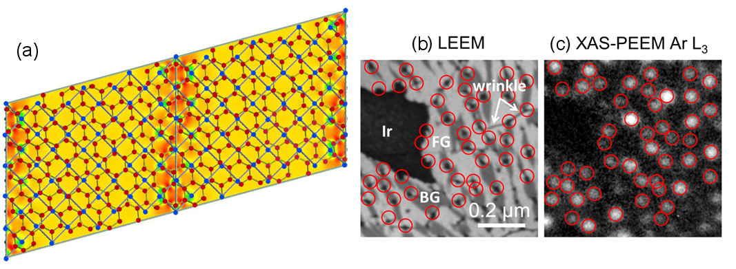
Figure 1: (a) Two contiguous unit cells of buckled graphene on Ir(001), as determined by ab initio calculations. (b) LEEM image of graphene/Ir(001) after Ar ion irradiation and subsequent annealing to 1050°C; the black dots correspond to Ar nanobubbles under graphene. (c) XAS-PEEM image of the same region. The intensity of the resulting image is proportional to the Ar concentration, with the bright regions corresponding to Ar clusters.
[1] A. Locatelli et al., ACS Nano 7, 6955 (2013).
[2] G. Zambrolini et al., Nano Lett. 15, 6162 (2015).
[3] These authors, in preparation.
Invited
Imaging strain waves in a PhotoEmission Electron Microscope: Magnetism goes surfing
1ALBA Synchrotron Light Source, Spain
2Institut de Ciència de Materials de Barcelona (ICMAB-CSIC), Spain
3Dept. of Condensed Matter Physics, University of Barcelona, Spain
4Institut für Physik, Johannes Gutenberg Universität Mainz, Germany
5Swiss Light Source, Paul Scherrer Institut, Switzerland
6Paul-Drude-Institut fur Festkörperelektronik, Germany
Surface Acoustic Waves (SAWs) are propagating Raleigh waves in the upper micrometric layer of a crystal, which propagate large distances and can be generated in piezoelectric materials by applying RF electric fields to transducer electrodes on the surface. We have shown that it is possible to image such waves in LiNbO3 by X-ray PhotoEmission Electron Microscopy (XPEEM), since it is sensitive to the piezoelectric part of the SAW. Thus, the effect of fast strain changes on structures grown on LiNbO3 can be studied with temporal resolution below 100 ps and up to 50 nm spatial resolution, offering a novel approach for studies of dynamic strain in a wide range of research fields (crystallography, nanoparticle manipulation, chemical reactions, magnetism…) The application to the study of dynamic magneto-elastic effects in Ni microstructures will be presented. The magneto-elastic effect or inverse magnetostriction (i.e., the change of magnetic properties caused by an elastic deformation) has attracted much interest due to its potential to write small magnetic elements by an electric voltage rather than current, avoiding energy losses. However, so far practical demonstrations were realized on timescales far too slow for most applications. Combining XPEEM with XMCD magnetic contrast we have imaged the Ni magnetic states at the different phases of the SAW, demonstrating that the strain-driven magnetic anisotropy changes on the sub-nanosecond timescale are as efficient as for the static strain case. Different delays (100-300 ps) of the magnetic response to the strain wave were measured, depending on the magnetic configuration. The delays are related to the intrinsic magnetization dynamics of the Ni patterns. Thus it is shown that while the magneto-elastic effect itself is very fast, for the speed of a potential device the magnetization state has to be properly designed.
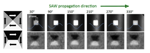
Figure 1: Left, top: Scheme of magnetic domains in a Ni square without net anisotropy, forming a Landau flux closure state (arrows indicate magnetic directions and gray color contrast in XMCD-PEEM). Left, bottom: domain configuration if an additional uniaxial magnetic anisotropy is induced, favoring horizontal magnetization (black and white domains). Right, top: Series of direct images taken with different respective positions of the strain wave and a Ni square (2 µm side). The square is in the maximum of the strain wave (white zone) between the images of 150° and 210° and in the minimum between 330° and 30°. Right, bottom: Corresponding images with XMCD magnetic contrast showing the magnetic domains in the Ni square.
[1] M. Foerster et al., arXiv:1611.02847.
Contributed talk
Magnetic domains on magnetite islands: from XMCD-PEEM to micromagnetism
1Instituto de Química Física "Rocasolano", Madrid, 28006, Spain
2Dpto. De Física de Materiales, Universidad Complutense de Madrid, Madrid 28040, Spain
3Unidad Asociada UMC-IQFR(CSIC), Madrid 28006, Spain
4Instituto de Cerámica y Vidrio (CSIC), Madrid 28049, Spain
5Alba Synchrotron Light Facility, CELLS, Barcelona E-08290, Spain
6Dpto. de Física Aplicada, Universidad Autónoma de Madrid, Madrid 28049, Spain
7Instituto de Ciencia de Materiales de Madrid, CSIC, Madrid E-28049, Spain
Magnetite nanostructures and thin films have been grown in spintronic devices such as spin valves in order to take advantage of the high Curie temperature, stability, and predicted half-metal character. However, thin films present magnetic properties which are rather different from the properties of bulk magnetite: high coercive fields, high saturation fields, out-of-plane magnetization, superparamagnetism in ultrathin films, or unexpected easy-axes. An explanation for these effects are growth defects, among which antiphase domain boundaries (APBs) are the best example. In the present work, we study the magnetic domains on flat single-crystal magnetite and other mixed spinels grown on Ru(0001) by molecular beam epitaxy [1,2]. As each island grows from a single nucleus, there are expected to be free of APBs. We have measured with nanometer-resolution the 3D magnetization of the islands by combining x-ray magnetic circular dichroism images acquired in a photoemission electron microscope at different azimuthal angles. The 3D magnetization maps have been used as the initial magnetization configuration for micromagnetic simulations of islands with the same lateral and vertical dimensions as the experimental ones. The Mumax3 software has been used to perform the micromagnetic simulations. By comparing the evolution of the micromagnetic simulations with the experimental behavior of the islands after annealing, we seek to validate the material parameters that define their magnetic behavior and to identify cases where defects or other effects play a role.
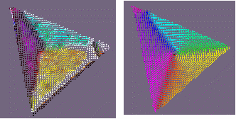
Figure 1: Left: experimental magnetization in a magnetite island as determine by XMCD-PEEM. Right: micromagnetic simulation using as a starting configuration the experimental one.
[1] M. Monti et al., Phys. Rev. B 85, 020404 (2012).
[2] L. Martín-García et al., Adv. Mat. 27, 5955 (2015).
[3] A. Vansteenkiste et al., AIP Adv. 4, 107133 (2014).
Contributed talk
Ultrafast LEED: Exploring surface dynamics with short electron pulses
1IV. Physical Institute - Solids and Nanostructures, University of Göttingen, Germany
2International Center for Advanced Studies of Energy Conversion (ICASEC), University of Göttingen, Germany
3Institute for Experimental and Applied Physics, University of Kiel, Germany
Low-energy electron diffraction (LEED) is one of the prime techniques of surface science, allowing for detailed insights into a variety of phenomena such as structural phase transitions, surface reconstructions or chemical reactions [1]. Yet, many of these features exhibit highly-complex couplings and correlations between the electronic, magnetic and structural degrees of freedom, which are difficult to disentangle using steady state analyses of systems in equilibrium. While the electronic and spin systems are already extensively studied at surfaces on their intrinsic timescales, gaining experimental access to ultrafast structural evolution remains challenging. Hence, in order to reach a comprehensive and quantitative understanding of ultrafast dynamics at surfaces, a time-resolved implementation of LEED is highly desirable.
Here, we present the development of ultrafast low-energy electron diffraction (ULEED), employing low-energy electron pulses in a laser-pump/electron-probe scheme. Within this approach, a laser-triggered nanoscopic needle emitter is utilized in a miniaturized electrostatic lens geometry as a high-brightness source. The resulting electron pulses exhibit a minimal duration down to 1 ps at the sample for electron energies of 20-200 eV.
We demonstrate the potential of ULEED by investigating the optically induced transition between charge density wave (CDW) phases at a single-crystalline 1T-TaS2 surface [2,3]. We also apply ULEED to study the dynamics of adsorbates on metal surfaces.
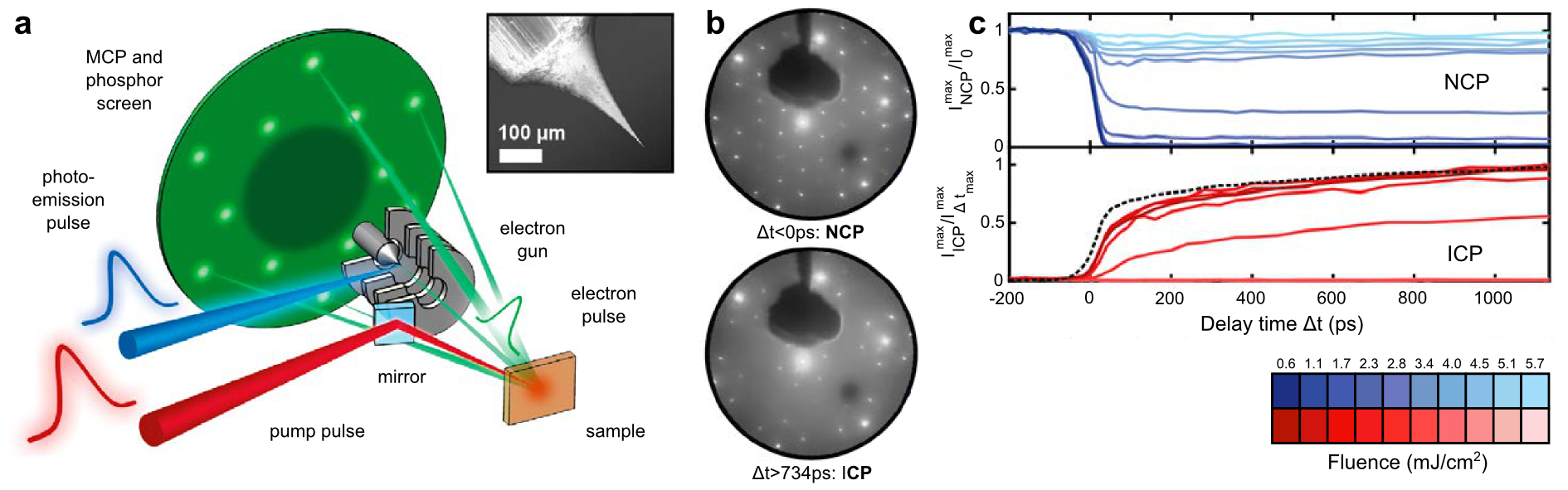
Figure 1: Ultrafast LEED: a) Experimental setup; b) Diffraction images of 1T-TaS2 taken before and shortly after optical excitation reveal the ultrafast transition between CDW phases; c) Temporal evolution of CDW spot intensities.
[1] M.A. Van Hove, W.H. Weinberg and C.-M. Chan, Low-Energy Electron Diffraction, Springer Verlag, Heidelberg (1986)
[2] S. Schweda et al., International Conference on Ultrafast Phenomena, paper UTh2B.3, OSA (2016)
[3] S. Vogelgesang et al., in preparation
Contributed talk
Steering the growth of multiple ordered heteromolecular phases by utilizing intermolecular repulsion
1Peter Grünberg Institut (PGI-3), Forschungszentrum Jülich, 52425 Jülich, Germany
2Jülich Aachen Research Alliance (JARA)-Fundamentals of Future Information Technology
The interfaces between organic semiconductors and metals have been investigated intensively in order to improve and develop future electronic devices. In this context the formation of molecular blends (i.e., heteromolecular layers containing at least two different types of molecules, usually charge donors und acceptors) on metal surfaces is of great interest. Many different techniques have been applied in the past to investigate different prototypical systems.
In this presentation, we report a novel thermodynamic phase diagram for molecular blends formed in submonolayers [1]. In a comprehensive LEEM study on PTCDA+CuPc on Ag(111) we find five crystalline phases (two homo- and three heteromolecular structures) having different stoichiometry. Large eutectic regions exist in the phase diagram, caused by the opposite intermolecular interaction of its components - repulsive for CuPc, attractive for PTCDA. We find that the repulsive species forms a two-dimensional lattice gas, the density of which determines the stability of all other crystalline phases. The existence of critical gas-phase densities is the basis for understanding the constant-volume phase diagram that perfectly describes our experimental observations. We anticipate the general validity of this type of phase diagram for binary systems containing 2D gas phases, and emphasize that the density of the gas phase allows engineering of the interface structure.In this presentation, we report a novel thermodynamic phase diagram for molecular blends formed in submonolayers [1]. In a comprehensive LEEM study on PTCDA+CuPc on Ag(111) we find five crystalline phases (two homo- and three heteromolecular structures) having different stoichiometry. Large eutectic regions exist in the phase diagram, caused by the opposite intermolecular interaction of its components - repulsive for CuPc, attractive for PTCDA. We find that the repulsive species forms a two-dimensional lattice gas, the density of which determines the stability of all other crystalline phases. The existence of critical gas-phase densities is the basis for understanding the constant-volume phase diagram that perfectly describes our experimental observations. We anticipate the general validity of this type of phase diagram for binary systems containing 2D gas phases, and emphasize that the density of the gas phase allows engineering of the interface structure.
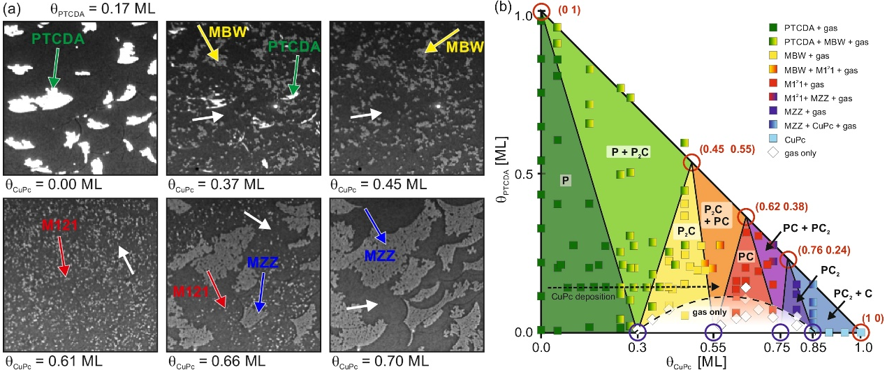
Figure 1: (a) Bright-field LEEM images recorded during a binary deposition experiment: Initially, 0.17 ML of PTCDA form islands on the Ag(111) surface (upper left image). The following LEEM images were recorded during subsequent CuPc deposition of 0.7 ML. The PTCDA islands (marked green) are sequentially transformed into MBW (yellow), M121 (red) and MZZ islands (blue), according to the stoichiometry sequence. (b) Corresponding phase diagram for the submonolayer regime: Data points and colored areas mark the regimes of pure and eutectic phases as obtained from experiment and thermodynamic model, respectively. The path of the experiment shown in (a) is indicated by a dotted black arrow. The model is based on more than 20 LEEM experiments with different initial coverages. Abbreviations: P = PTCDA, C = CuPc; Sequence and stoichiometry of the phases: PTCDA (P) - MBW (P2C) - M121 (PC) - MZZ (PC2) - CuPc (C).
[1] C. Henneke, D. Schwarz, F.S. Tautz, C. Kumpf, Nature Materials, in press, DOI: 10.1038/NMAT4858
Invited
Curved crystal surfaces: A playground for general surface concepts and dimensionality transitions
1Instituto de Ciencia de Materiales de Aragón (ICMA) and Departamento de Física de la Materia Condensada, CSIC-Universidad de Zaragoza, Zaragoza, Spain
Crystal surfaces with a small deviation from a high symmetry plane have enormous potential for surface science research and applications. Such "vicinal" planes, characterized by arrays of atomic steps, exhibit distinct chemical and electronic properties, and are useful templates to achieve uniaxial symmetry and single azimuthal domains in epitaxial layers, or to drive self-organized nanostructure growth.
A way of systematically studying step-related phenomena is to use curved crystals. The beauty of these special substrates is that they integrate all vicinal directions, which are accessible by scanning the source beam or tip along the curvature of the crystal. In this way, the sample provides a smooth variation of the step density that is directly related to a terrace width variation from sub-micron to the nanometer range.
These samples has allowed us to revisit old and to explore new surface science problems [1-3]. I will discuss step-lattice interactions, scattering of surface states and growth. Our experiments demonstrate the immense power of the curved surface approach, which allows one to directly image fine physical-chemical properties of surface systems, such as to settle controversial issues and to unveil new phenomena.
Figure 1: (a) Example of three curved crystals: c-Au(111), c-Cu(111) and c-Ag(111). (b) Example of a 2D to 1D electronic transition taking place in Bi(111) under the presence of a high density of steps.
[1] J.E. Ortega et al., Physical Review B 87, 115425 (2013).
[2] A.L. Walter et al., Nature Communications 6, 8903 (2015).
[3] L.A. Miccio et al., Nanoletters 16, 2017 (2016).
Invited
Mapping Enantioselectivity across Surface Structure Space
1Dept. of Chemical Eng.
2W.E. Scott Institute for Energy Innovation, Carnegie Mellon Univ., 5000 Forbes Ave., Pittsburgh, PA 15213
Enantioselectivity can be observed on naturally chiral metal surfaces with structures that are described as having flat low Miller index terraces separated by kinked step edges, therefore lacking mirror symmetry. This work has mapped the enantiospecific decomposition kinetics of tartaric acid (TA) on ~500 different single crystal planes exposed by the surfaces of Cu(111) and Cu(100) Surface Structure Spread Single Crystal (S4C). S4Cs are single crystals polished into a spherical shape that expose continuous distributions of surface orientations vicinal to primary orientation [1]. The left hand panel of the figure shows a Cu(111) S4C with a curved surface exposing all crystal faces having orientations lying within ~10o of Cu(111). During isothermal decomposition, XPS has been used to map the temporal evolution of the coverage of TA at points across the Cu(111) and Cu(100) S4Cs. The center and right hand panels of the figure shows D- and L-TA coverage maps across the Cu(100) S4C following heating at 450 K to decompose ~70% of the initially adsorbed TA. Blue reveals regions in which the TA has been completely decomposed. Red reveals regions in which TA decomposition has barely begun. The fourfold symmetry of the Cu(100) substrate is apparent, and the enantiospecificity of the decomposition kinetics is revealed by the spiral nature of the two maps and their opposite sense of handedness for D- and L-TA. These data can be analyzed to yield the enantiospecific rate constants for TA decomposition as functions of surface orientation.
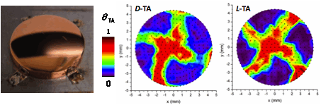
[1] A. de Alwis, B. Holsclaw, V.V. Pushkarev, A. Reinicker, T.J. Lawton, M.E. Blecher, E.C.H. Sykes, AJ. Gellman, Surface Science 608, 80-87 (2013).
Contributed talk
Benchmarking DFT calculations for metal oxides: geometric adsorption site of copper and silver adatoms on magnetite
1Diamond Light Source, Oxfordshire, UK
2University of Vienna, Austria
3Technical University of Vienna, Austria
4Technical University of Munich, Germany
Single-site catalysis is a promising field for pursuing model catalytic reactions, with the objective of one day designing catalysts from the bottom up. However, in order to gain true insight into the inner workings of any system, it is necessary to be able to reliably theoretically model it. Thus to benchmark such theoretical calculations it is of the utmost importance to acquire stringent quantitative experimental constraints. In this work we utilize the quantitative geometric structure, determined by normal incidence X-ray standing wave (NIXSW), as a benchmark for density functional theory (DFT) calculations of one such promising single site catalyst: dispersed single adatoms on the (001) termination of magnetite.
The recently elucidated surface reconstruction of Fe3O4(001)[1] patterns the formation of well separated single adatoms with a comparatively high coverage[2]. However, although the surface structure is well known [1], the geometry of the adatoms has only been probed by non-quantitative techniques such as STM and XPS, which do not provide suitable benchmarks for theoretical calculations, providing a fertile field for a NIXSW study.
We specifically probed the surface structure silver (Ag1) and copper (Cu1) adatoms, which are predicted to occupy the same lateral site, but dramatically different vertical heights. NIXSW triangulation measurements, utilising the (400), (440) and (311) reflection planes, identified that both adatoms do indeed occupy the same lateral site, specifically bridging two surface oxygen atoms, at an adsorption height of 0.43±0.03 Å and 0.96±0.03 Å respectively, as shown in Figure 1. Theoretical calculations, in which the lattice constant was correctly modelled, predicted that Ag1 and Cu1 lay 0.89 and 0.41 Å above the projected bulk termination, in good agreement with the experimental results. However, theoretical models that overestimated the lattice constant underestimated the adsorption height, exemplifying the necessity to accurately model the whole system.
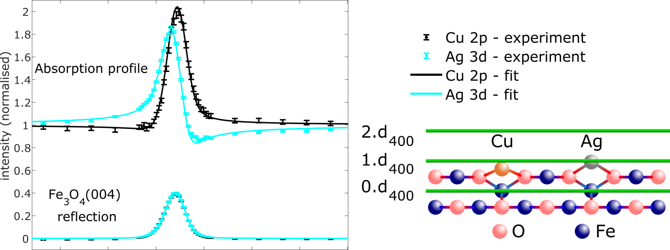
Figure 1: (left) Cu 2p and Ag 3d NIXSW from the (400) reflection of Fe3O4(001) and (right) the resulting difference in adsorption height of Cu1 and Ag1 with respect to the (400) spacing of the magnetite. Scanning tunneling microscopy image of the dimer of cyclized products (inset) and the associated calculations on Bader charge distribution, evidencing the strongly polarized bonds responsible for the attractive dipole-dipole interaction.
[1] R. Bliem, et al., Science 346, 1215 (2014).
[2] Z. Novotný, et al., Physical Review Letters 108, 216103 (2012).
Contributed talk
Adsorbate Phases and Structural Evolution Upon Reduction of Quasi One-Dimensional CoO2 Chains on Ir(100)
1Solid State Physics, Friedrich-Alexander University Erlangen-Nuremberg, Erlangen, Germany
2Division of Synchrotron Radiation Research, Lund University, Sweden
On the Ir(100) surface one can prepare highly ordered, quasi one-dimensional, transition metal oxide chains in a (3×1) superstructure [1]. These oxide chains have an unusual MO2 stoichiometry in which the metal atom (M = Mn, Fe, Ni, Co) is decoupled from the iridium substrate (Figure 1a). Using the example of CoO2 chains we analyze structural changes and phases upon adsorption and reaction with reducing species like H2 and CO in an UHV environment. Due to the long-range order of the system before and after the reactions it is possible to quantify these structural changes by means of high-precision, full-dynamical LEED analyses. Combining the detailed structural information with data obtained by HR-XPS, STM, TDS, and supporting DFT calculations we are able to follow the processes during the reactions on the atomic scale.
Oxidation of H2 and CO and in consequence reduction of the CoO2 chains eventually to a well-ordered (3×1) Ir2Co surface alloy may be thermally activated near room temperature. As evidenced by HR-XPS spectra, the reaction with H2 proceeds via the formation of an intermediate OH-species on the surface. In the case of reduction by CO the formation of CO2 proceeds from a ordered c(6×2)-(CoO2+CO) adsorbate phase in which CO occupies an Ir bridge site (Figure 1b). An intermediate carbonate or other species cannot be detected. In the case of CO oxidation the initially high reaction rate is reduced because the CO molecules assemble on the freshly formed Ir2Co alloy and hence are spatially separated from the remaining intact or partially reduced cobalt oxide chains.
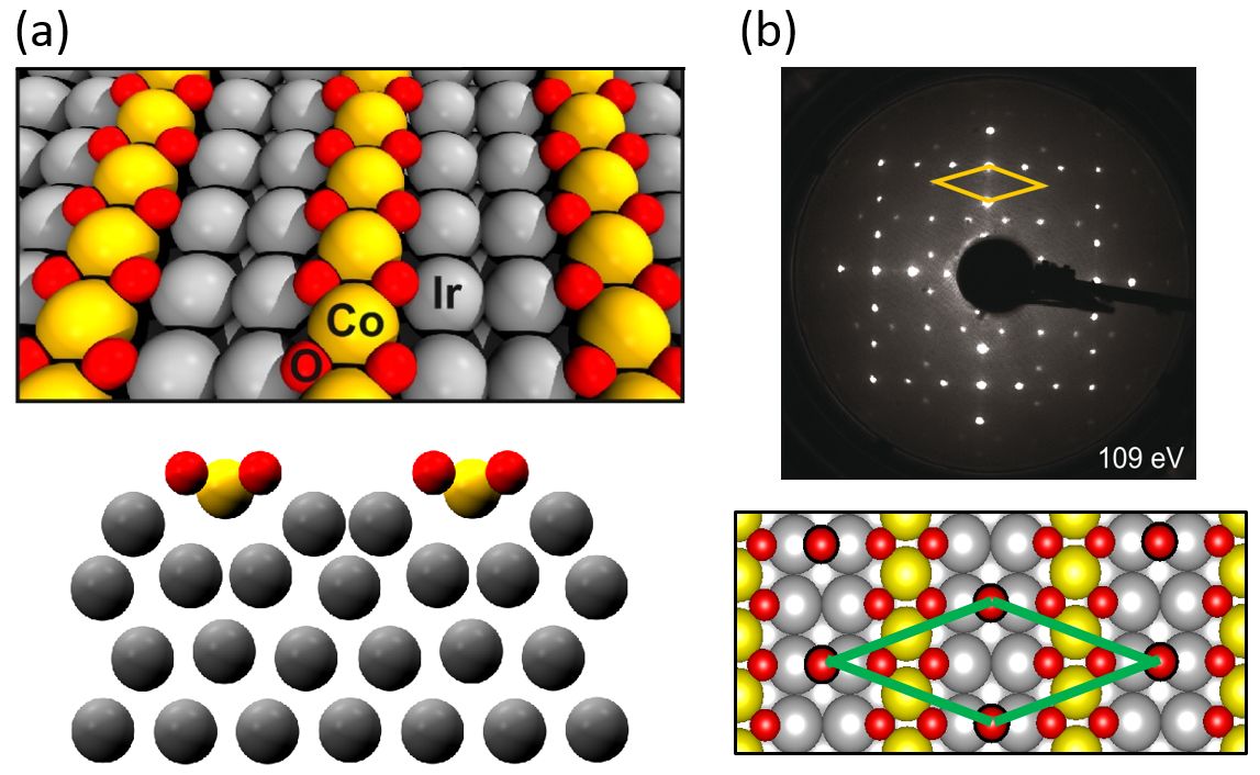
Figure 1: (a) (3×1)-CoO2 chain structure on Ir(100) and (b) c(63×2) CO adsorbate phase on the CoO2 chain structure with best-fit models as determined of the LEED structural analyses. Pendry R-factors (a) Rp = 0.10, (b) Rp = 0.13 .
[1] P. Ferstl et al., Phys. Rev. Lett. 117, 046101 (2016)
Invited
Quasicrystals and approximants in two-dimensional perovskite oxides
1Institute of Physics, Martin-Luther-Universität Halle-Wittenberg, Halle, Germany
2Max-Planck-Institut für Mikrostruktruphysik, Halle, Germany
When approaching the two-dimensional limit, oxides are known to exhibit strong variations in their structures and properties as compared to the respective bulk materials [1]. One of the extreme examples are the two-dimensional oxide quasicrystals (OQCs), which have been discovered for reduced perovskite oxides at the Pt(111) interface [2, 3]. OQCs have been reported for BaTiO3 and more recently also for SrTiO3. Furthermore, approximant structures have been observed, in which selected motifs of the OQC are periodically repeated. In Figure 1a an example of a simple approximant structures is given, which has been observed for BaTiO3 [4]. The more complex approximant structure shown in Fig. 1b has been reported for SrTiO3 [3]. The later is almost indistinguishable from the aperiodic structure in an diffraction experiment. Our studies unravel OQCs as best-controlled QC model systems for addressing the fundamental questions related to the driving forces for aperiodic structure formation.
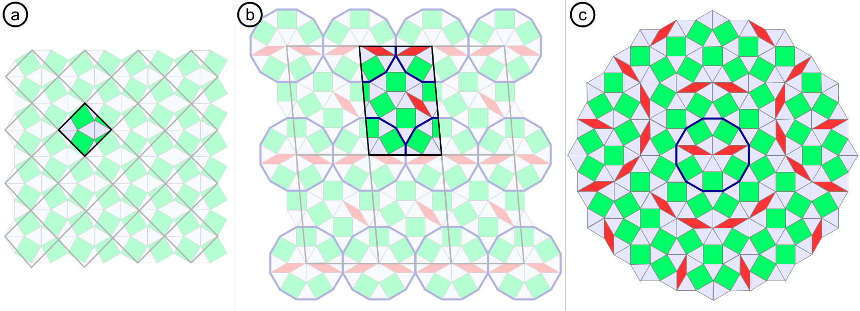
Figure 1: Comparison of periodic approximant tilings (a, b) and the aperiodic Stampfli-Gähler tiling as observed for OQCs (c). The OQC tiling lacks translational symmetry.
[1] F. Netzer, S. Fortunelli (eds), Oxide Materials at the two-dimensional limit, Springer (2016).
[2] S. Förster, K. Meinel, R. Hammer, M. Trautmann, W. Widdra, Nature 502, 215 (2013).
[3] S. Schenk et al., J. Phys.: Condens. Matt. doi.org/10.1088/1361-648X/aa5bdb (2017).
[4] S. Förster et al., Phys. Rev. Lett. 117, 095501 (2016).
Invited
Biphase ordering at Fe oxides
1Instituto de Ciencia de Materiales de Madrid (CSIC), Spain
2Chalmers University of Technology, Gothenburg, Sweden
The phase diagram of oxide surfaces and ultrathin films may be different from that of their bulk counterparts, and binary Fe oxides provide very good examples. In the O-poor limit, their bulk phase diagram includes the antiferromagnetic rock-salt insulator FeO and the ferrimagnetic spinel half-metal Fe3O4. FeO is not stable at ambient conditions but with a significant number of Fe vacancies that resemble Fe3O4 inclusions [1]. However, a single FeO(111) monolayer has been stabilized on different substrates. Even a record thickness of 8 nm preserving the 1:1 stoichiometry has been achieved under ultra-high vacuum conditions, before the film evolves to Fe3O4 [2]. A more intriguing phenomena emerges when the two distinct phases coexist at the same termination (biphase ordering), as has been observed at the surface of Fe3O4 [3].
Here we will show that at the origin of this behavior lies the tendency of FeO(111) to introduce tetrahedrally coordinated Fe sites. Together with the reduced energy difference between FeO and Fe3O4 in the ultrathin limit, this favors the coexistence of both phases in the few monolayers regime, explaining the emergence of biphase ordering [4]. Furthermore, these findings provide interesting clues to solve the elusive Fe3O4 (111) surface structure.
Figure 1: Side view of the spinel-like and wurtzite terminations of FeO(111).
[1] I. Bernal-Villamil, S. Gallego, Phys. Rev. B 90, 195126 (2014)
[2] L. Martín-García et al., J. Mater. Chem. C 4, 1850 (2016)
[3] N.G. Condon et al., Phys. Rev. B 55, 15885 (1997)
[4] I. Bernal-Villamil, S. Gallego, Phys. Rev. B 94, 075431 (2016)
Contributed talk
Nanostructured Aluminum Oxides and Metal Electrodeposition
1Division of Synchrotron Radiation Research, Lund University, SE-22100 Lund, Sweden
2MAX IV Laboratory, SE-22594, Lund, Sweden
3ESRF - The European Synchrotron, 71 Avenue des Martyrs, 38000 Grenoble, France
Traditional surface science studies have been quite successful in determining several surface structures for alumina films, in particular those grown on NiAl, where the bulk structure consists of a combination of several building blocks but the surface Al atoms are found to occupy sites with either tetrahedral or pyramidal coordination [1]. However, the naturally forming 'native oxide' layers are found to be largely amorphous. The thickness of this layer can be increased electrochemically, i.e. the industrial process of anodization, and to some extent the degree of crystallinity found depends on the applied voltage [2]. This type of oxide layer is called an anodic barrier layer and forms in neutral type electrolytes. In acidic electrolytes a porous oxide film is found, in which case the oxide has many nanometer sized pores and forms the base of most industrial aluminum coloring processes. Furthermore, under certain conditions these pores are found to be self-ordering [3]. They form hexagonal arrays and the pore diameter can be tuned by changes in potential, making excellent nanoscale templates.
We have investigated the formation and self-ordering behavior of porous type anodic alumina films in operando using Grazing Transmission Small-Angle X-Ray Scattering (GTSAXS). The experimental setup and scattering geometry is illustrated in Fig 1A and Fig. 1B. We observe the that the in-plane arrangement of the nanopores is independent of substrate crystallographic orientation whereas the oxide growth rate is not. The self-ordering behavior is studied in a variety of electrolytes and at several potentials. It is also possible to follow the chemical etching of the oxide (pore widening) and subsequent metal deposition within the nanopores. The experimental approach presented can be applied to the study of a large variety of electrochemically produced materials such as magnetic nanowires, novel solar cell designs and catalysts.
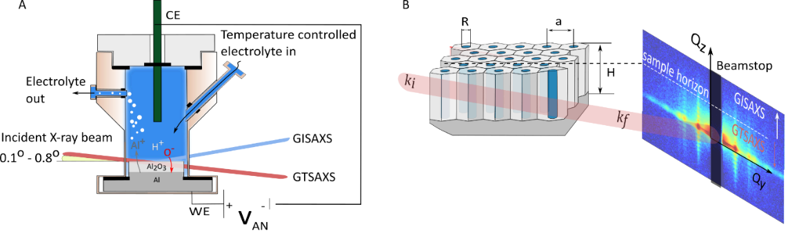
Figure 1: Experimental Schematic. A) The electrochemical cell used for in operando experiments. B) scattering geometry and an example scattering pattern.
[1] G. Prevot et al., Phys. Rev. B, 85, 205450 (2012)
[2] J.W. Diggle et al., Chem. Revs., 69(3), 365 (1969)
[3] H. Masuda, K. Fukuda, Science, 268, 1466-1468 (1995)
Invited
Can dynamic force microscopy really "see" intermolecular bonds?
1School of Physics and Astronomy, University of Nottingham, Nottingham NG7 2RD, UK
2Physics Department and Materials Science Institute, Lancaster University, Lancaster, LA1 4YB, UK
3Institute for Interdisciplinary Research Jianghan University Wuhan 430056 China
4Department of Physics, King's College London, Strand, London WC2R 2L, UK
Since Gross et al.'s pioneering observation of the internal "architecture" of a pentacene molecule in 2009 [1], there has been a rapid growth in ultrahigh resolution imaging of single molecules using dynamic force microscopy [2]. Image interpretation is, however, always a challenge with any type of scanning probe technique as, very often, the precise role of the probe can be difficult to 'deconvolve' from the experimental data. I shall discuss a series of ultrahigh vacuum, low temperature force microscopy results (based around the qPlus sensor [3]) for a variety of molecules adsorbed on both metal and semiconductor surfaces: NTCDI [4,5] and biisonicotinic acid (which are both largely planar), and C60 (which is, of course, very far from planar) [6].
Although the biisonicotinic acid data (see Fig. 1) were acquired with a CO-terminated tip, as per the standard approach in the dynamic force microscopy community, high resolution imaging of both NTCDI and C60 involved imaging using a tip which, to the very best of our knowledge, was terminated by an NTCDI or C60 molecule respectively. Intramolecular resolution was possible for tips that interacted both very strongly (~ 2 nN) and very weakly (~ 50 pN) with the Si(111)-(7×7) surface, demonstrating that an inert probe is not a prerequisite for intramolecular imaging. This has important implications for the continuing development of 'internal' imaging of adsorbed molecules on semiconductors.
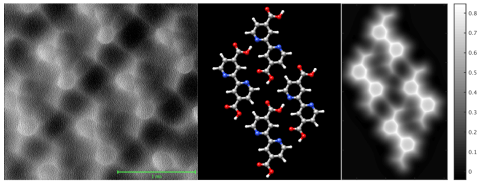
Figure 1: (L-R) Experimental constant height frequency shift image of a monolayer of biisonicotinic acid on Au(111); geometry-optimized structure of the biisonicotinic assembly (determined using the CP2K DFT code [7]); constant height image simulated using the analytical model developed by Hapala et al. [8]
[1] L. Gross et al., Science 325, 1110-1114 (2009)
[2] N. Pavliček and L. Gross, Nature Rev. Chem. 1, 0005 (2017)
[3] F.J. Giessibl, Rev. Mod. Phys. 75 949 (2003)
[4] A. Sweetman et al., Nature Comm. 5, 3931 (2014)
[5] A. Sweetman et al., Phys Rev B 90, 165425 (2014)
[6] S.P. Jarvis et al., Phys Rev B 92, 241405(R) (2015)
[7] https://www.cp2k.org/
[8] P. Hapala et al., Phys Rev B 90, 085421 (2014)
Contributed talk
Structure determination of individual non-planar molecules by means of nc-AFM with functionalized tips
1Institute of Experimental and Applied Physics, University of Regensburg, 93053 Regensburg, Germany
2Physik Department E20, Technische Universität München, 85748 Garching, Germany
3IBM Research-Zurich, 8803 Rüschlikon, Switzerland
4Karlsruhe Institute of Technology (KIT), 76344 Eggenstein-Leopoldshafen, Germany
Functionalizing the tip of an AFM with a single CO molecule allows for unambiguous structure determination of individual molecules [1]. This technique was widely applied for different molecules [see e.g. 2]. However, the molecules under investigation exhibited manly planar structures, adsorbed parallel onto the sample surface and showed no internal degrees of freedom.
Here, we present experimental results obtained with a combined STM/AFM operated at low temperatures in UHV. We show two routes for structure determination of individual molecules by means of nc-AFM with CO functionalized tips for molecules that could not be identified from conventional scanning probe imaging:
In the first case, we determine the entire 3D geometry of a helically shaped diphenanthrene derivate. To do so, we record a time-demanding, full 3D dataset in a safe but sufficiently close distance regime [3]. To analyse the molecular geometry we display the AFM signal along different planar cross sections of the 3D data [4].
In the second case, we analyse subtle differences in the 3D structure of free-base and metallated porphyrin derivates adsorbed on Cu(111) [5]. Since unambiguous molecular identification is not possible in conventional imaging we record AFM data in a close but safe distance range by introducing vertical imaging - that is recording the frequency shift in a plane perpendicular to the sample surface. These images allow unambiguous molecular species identification. Moreover, mapping the minimum position of the frequency shift [6] within these vertical images, we quantify the vertical movement of the central metal atom upon tip induced conformational switching of one of the porphyrin derivates.
[1] L. Gross et al., Science 325, 1110 (2009).
[2] S. Jarvis et al., Int. J. Mol. Sci. 16, 19936 (2015).
[3] F. Mohn et al., Appl. Phys. Lett. 99, 053106 (2011).
[4] F. Albrecht et al., J. Am. Chem. Soc. 137, 7424 (2015).
[5] K. Diller et al., J. Chem. Phys. 136, 014705 (2012).
[6] B. Schuler et al., Phys. Rev. Lett. 111, 106103 (2013).
Contributed talk
Demonstration of large converse piezoelectric effect on a single molecule
1Institute of Physics, Czech Academy of Sciences Prague, Czech Republic
2Regional Centre of Advanced Technologies and Materials, Faculty of Science, Department of Physical Chemistry, Palacky University, Olomouc, Czech Republic
33Institute of Chemistry and Biochemistry, Czech Academy of Sciences Prague, Czech Republic
The converse piezoelectric effect is a phenomenon, in which a mechanical strain is generated in a material due to an applied electrical field. Demonstration of the piezoelectric effect on nanoscale remains the challenge. In this work, we investigate the piezoelectric effect in single 2,17-Bis(acetylsulfanyl) heptahelicene (BA7H) molecules on Ag(111) surface, using the non-contact atomic force microscopy (AFM). The BA7H on the substrate forms circular and linear islands, which can be effectively disassembled to individual molecules by the AFM tip, to exclude collective influence on the piezoelectric measurements. We can reversibly flip the acetylsulfanyl group at the terminal of the molecule exposed to the tip between two metastable configurations via a controlled tip-molecule interaction. In addition, we characterized the bias-induced deformations of the BA7H molecules and found that the piezoelectric constant is independent of the acetylsulfanyl group conformation. Thereby this demonstrates that the piezoelectric effect is intrinsic to the helicene core. We corroborate the experimental evidence by the total energy DFT simulations. The calculations reveal strong charge transfer between BA7H molecule and the metallic substrate, which gives rise to a vertical electric dipole. The presence of the electric dipole coupled with a soft vibrational mode steaming from a helical structure of the molecule originates the strong piezoelectric effect.
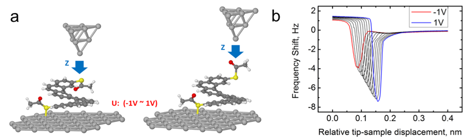
Figure 1: Sample graphics (B/W in print) Schematic view of a metallic tip approach over two different configurations of BA7H molecules. b) Bias dependent force-distance spectroscopy revealing strong variation of the tip-sample distance with applied bias, at which the molecule is contacted.
Contributed talk
On-surface synthesis and characterization of reactive molecules
1IBM Research-Zurich, 8803 Rüschlikon, Switzerland
2CIQUS and Facultad de Química, Universidad de Santiago de Compostela, Spain
3Department of Chemistry, University of Warwick, UK
Non-contact atomic force microscopy (AFM) with functionalized tips allows direct imaging of the structure of molecules [1]. This method has been realized as an ideal tool to compare reactants with products of thermally activated on-surface reactions [2]. Another possibility to initiate on-surface reactions is atomic manipulation using the tip of the microscope. Recently, we have followed the latter route to investigate molecules that are too elusive to be characterized by other methods [3].
Suitable precursor molecules are required in which individual bonds act as predetermined breaking points. These weakest bonds (for example, carbon-halogen or carbon-hydrogen bonds) can then be cleaved by atomic manipulation. Applying this versatile procedure opens a multitude of possibilities. For example, reactive intermediates like arynes can be characterized in unprecedented detail [4], reversible ring-opening and -closing reactions can be initiated and studied [5], or diradicals like triangulene can be generated which might be interesting for spintronic applications because of their unpaired electrons [6].
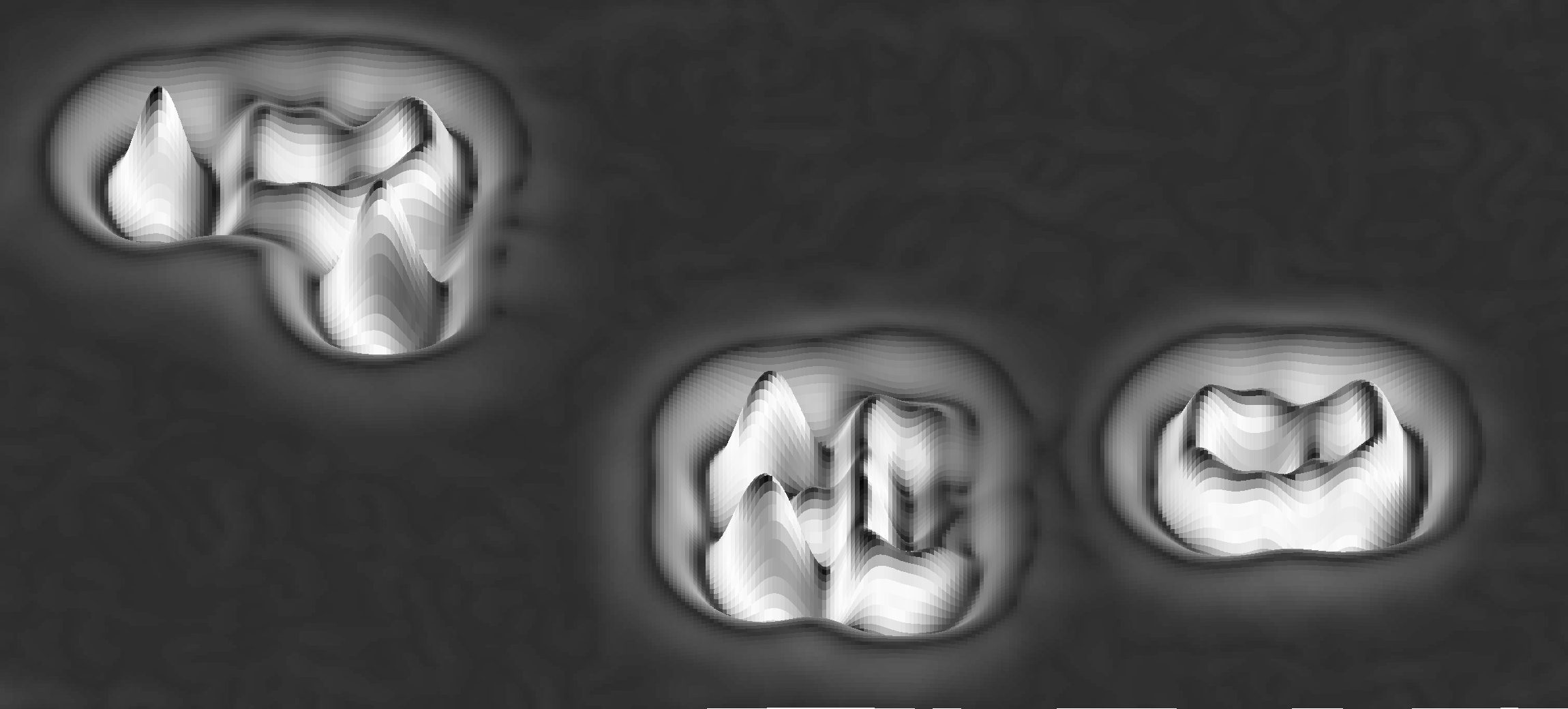
Figure 1: Pseudo three-dimensional rendering of an AFM image of three molecules generated by atomic manipulation with several Br atoms adsorbed close by.
[1] L. Gross et al., Science 325, 1110 (2009)
[2] D. G. de Oteyza et al., Science 340, 1434 (2013)
[3] N. Pavliček and L. Gross, Nature Reviews Chemistry 1, 0005 (2017)
[4] N. Pavliček et al., Nature Chemistry 7, 623 (2015)
[5] B. Schuler et al., Nature Chemistry 8, 220 (2016)
[6] N. Pavliček et al., Nature Nanotechnology, doi:10.1038/nnano.2016.305 (2017)