Keynote
Towards electronic devices using graphene nanoribbons
1CFM CSIC-UPV/EHU and DIPC, Paseo Manuel de Lardizabal 5, E-20018, San Sebastián, Spain
2ICMAB-CSIC, Campus de la UAB, E-08193 Bellaterra, Spain
3IKERBASQUE, Basque Foundation for Science, E-48013, Bilbao, Spain
In this talk, I will present some studies of prototype electron devices made out of graphene nanoribbons that we have recently performed in our group in San Sebastián. In collaboration with our experimental colleagues, we have studied the properties of armchair GNRs (AGNRs) doped and functionalized in different ways. In particular, we have studied 7-AGNRs periodically doped with boron pairs on Au(111), and compared our findings with scanning tunneling microscopy/spectroscopy (STM/STS) and angle-resolved photoemission (ARPES) data. Furthermore, it is possible to grow structures formed by pristine segments separated by regions doped with B pairs [1]. We have studied the properties of such boron defects as scattering centers for GNR electrons, and found that they provide large effective barriers for the propagation of electrons in the valence band (VB), but are nearly transparent for the immediately lower energy band (VB-1) due to the different symmetry of both bands. As a result, the VB gives rise to quantized levels in the pristine regions that are clearly identified (see the Figure), with a remarkable agreement between theory and experiment [1].
From a purely theoretical perspective, we have explored a prototype 4-terminal semiconducting device formed by two crossed AGNRs as a function of the intersection angle, stacking, inter-GNR separation, GNR width, and voltage. [2] Interestingly, when the AGNRs intersect at θ=60° electrons injected from one terminal can be split into two outgoing waves with a tunable ratio around 50% and with almost negligible back-reflection. The split electron-wave is found to propagate partly straight across the intersection region in one ribbon and partly in one direction of the other ribbon, i.e., in analogy of an optical beam splitter. We rationalize our findings with a simple model that suggests that electronic beam splitters can generally be realized with crossed GNRs.
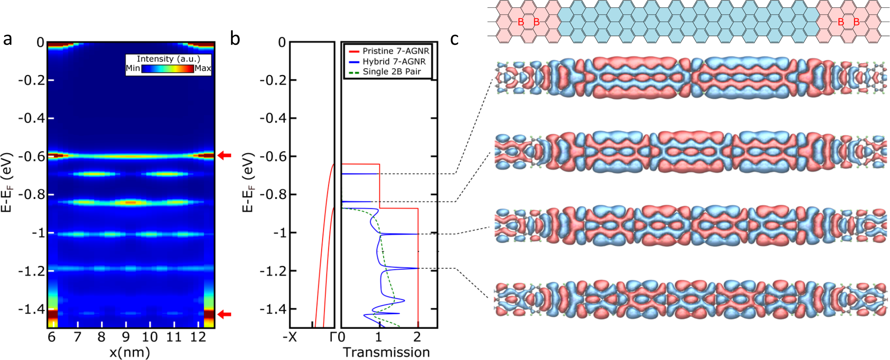
Figure 1: (a) Calculated projected density of states in a pristine segment between two borylated units 65Å apart. (b) Dispersion of the VB and VB-1 bands and the corresponding transmission curves for a pristine 7-AGNR (red line), a 7-AGNR containing an isolated B-pair defect (green doted line), and a 7-AGNR containing two B-pairs separated by 65Å (blue line exhibiting characteristic Fabry-Perot-like resonances). (c) Scheme and real part of the transmission eigenchannels with an increasing number of nodes as we move down in energy.
The authors acknowledge financial support from FP7 FET-ICT project No. 610446 project, EU H2020 project No. 676598, MINECO (Grant No. MAT2013-46593-C6-2-P), the Basque Dep. de Educación and the UPV/EHU (Grant No. IT-756-13).
[1] E. Carbonell-Sanroma, et al., Nano Letters 17, 50-56 (2017)
[2] P. Brandimarte, et al., J. Chem. Phys. 146, 092318 (2017)