

Invited
Structure and electronic properties of single-layer MoS2 on Au(111)
1Interdisciplinary Nanoscience Center (iNANO), Aarhus University, Denmark
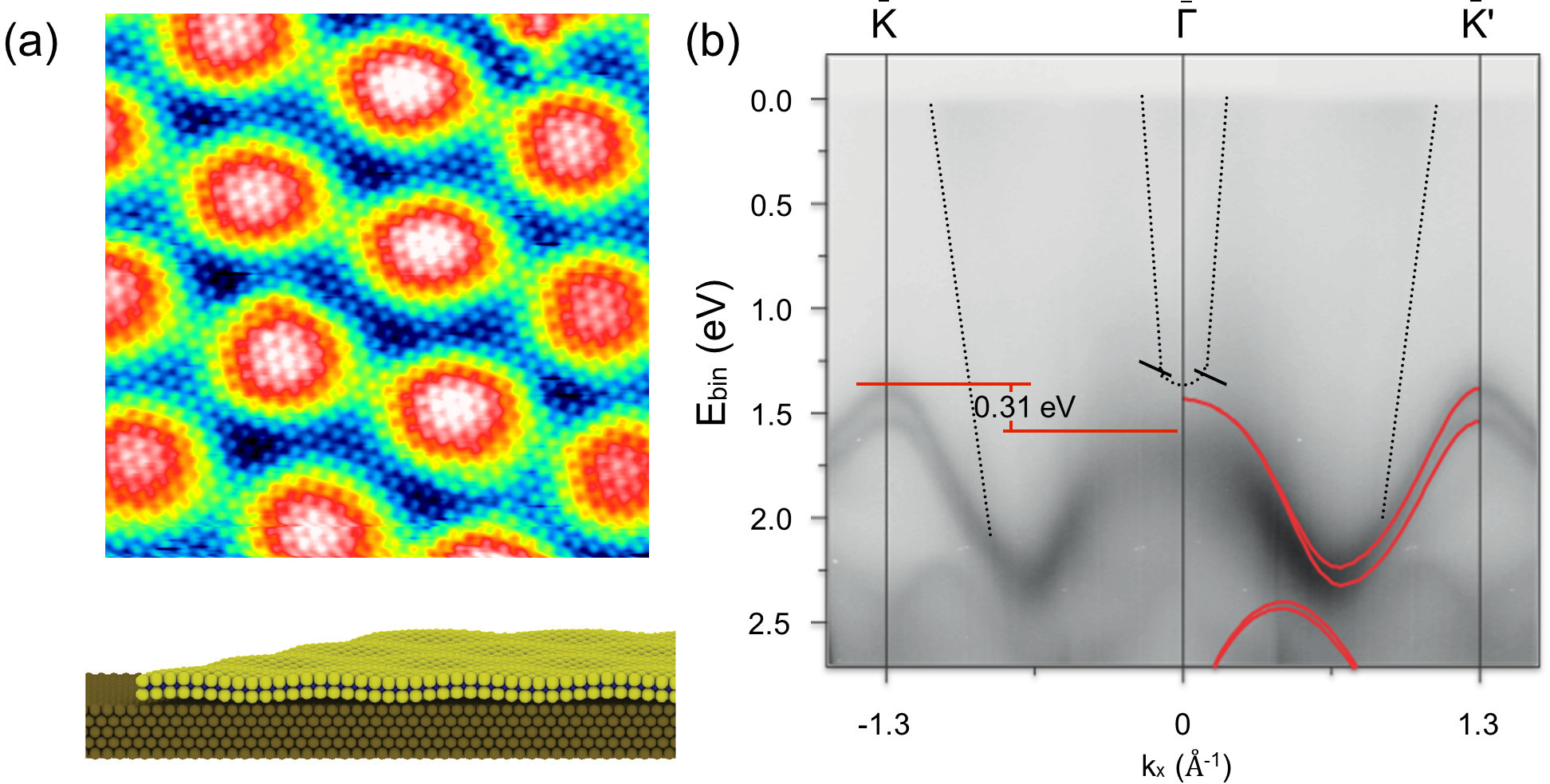
Single-layer MoS2 is one of the most studied of the two-dimensional transition metal dichalcogenides (TMDCs) as it was the first example of how a modified electronic structure reflected by a direct band gap and correspondingly different optical properties may develop when the TMDC becomes a single layer. Single-layer MoS2 can furthermore give rise to interesting new physics through the possibility of exploiting spin and valley degrees of freedom. We have developed a synthesis method that allows us to selectively form single-layer epitaxial MoS2 sheets grown with the (0001) basal plane in parallel to Au(111). This has the advantage of a well-defined and well-oriented system that enables us to systematically address the structural and electronic features pertaining to such single MoS2 layers on a metal support using scanning tunneling microscope (STM) and angle-resolved photoemission spectroscopy (ARPES). Coherent sheets of MoS2 at varying surface coverage can be formed by sequences of reactive physical vapor deposition of Mo in a H2S atmosphere followed by post annealing in the sulfiding atmosphere. Structurally, the single-layer MoS2 adopts a large characteristic superstructure due to the lattice mismatch, reflected by a moiré pattern in STM images [1,2]. Our DFT studies furthermore reveal that this modulation is influenced by the preferential bonding of the bottom S in the MoS2 sheet to on-top positions on the Au(111). The ARPES results [3] show that the Au-supported single-layer MoS2 retains the important direct band gap at the K point seen in free-standing single-MoS2, whereas the out-of-plane S bonding to Au leads to some distortions of the band near the Γ point. By varying the synthesis conditions we can furthermore study isolated MoS2 islands as well as stacking faults at the interface between MoS2 patches. This approach in particular allows us to address the edges terminating the MoS2 sheets, which are found in photoemission and STM studies to be metallic due to the presence of edge states in contrast to the semiconducting basal plane

Figure 1: (a) Atom-resolved STM image showing the atomic lattice and moiré pattern of MoS2/Au(111) (b) Photoemission results along the Γ-K direction for MoS2/Au(111).
[1] S.G. Sørensen, H.G. Füchtbauer, A.K. Tuxen et al., ACS Nano 8, 6788 (2014).
[2] S.S. Grønborg, S. Ulstrup, M. Bianchi et al., Langmuir 31, 9700 (2015).
[3] J.A. Miwa, S. Ulstrup, S.G. Sørensen et al., Phys. Rev. Lett. 114, 046802 (2015).