
Invited
In-situ atomic-scale investigation of CVD-grown graphene on polycrystalline nickel substrates
1IOM-CNR Laboratorio TASC, Area Science Park, s.s. 14 km 163.5, Basovizza, 34149 Trieste, Italy
2The Abdus Salam International Centre for Theoretical Physics, Strada Costiera 11, 34151 Trieste, Italy
3Department of Physics, University of Trieste, Via Valerio 2, 34127 Trieste, Italy
The understanding of growth mechanisms, at the atomic level and on substrates suitable for scalable CVD production, is a key step for the use of graphene in industrial applications. However, most studies so far are based on the interpretation of post-growth experiments on model surfaces, which can sometimes be misleading.
By means of variable-temperature scanning tunnelling microscopy, we studied the graphene growth process in the 380-500°C temperature range with a time resolution down to 100 ms/image and on commercially available polycrystalline Ni substrates. (111) and (100) facets were identified in the examined regions of the polycrystalline sample and growth mechanisms were investigated on both flat (100) terraces and highly-stepped regions. On flat terraces, graphene can grow directly on top of the metal or via in-plane carbide conversion, as already evidenced in our previous work on model (111) substrates [1]. On (100) grains, a variety of moiré superstructures are present, which can be well explained in atomistic models by the mismatch with the substrate and whose appearance in the STM images is well reproduced by density functional theory simulations. These moiré structures were found to be able to influence carbide segregation under graphene, thus providing a new route to tune its electronic properties on a nano-meter scale. Furthermore, with the aid of an add-on FAST module allowing for the acquisition of STM time-series up to video rate, novel growth mechanisms at stepped areas are unveiled, which rationalize the continuity of the graphene layer even when it lies on highly stepped polycrystalline substrates.
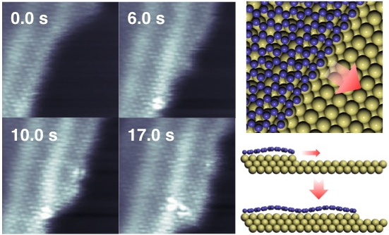
Figure 1: Graphene growth on (100) Ni facets. Left: selected frames of an atomically resolved Fast-STM movie during growth at 450°C; Right: atomistic model of the mechanism imaged on the left
[1] L.L. Patera et al., ACS Nano 7, 7901-7912 (2013).